The power line fluctuations and cut-offs cause damages to electrical appliances connected to the line. It is more serious in the case of domestic appliances like fridge and air conditioners. If a fridge is operated on low voltage, excessive current flows through the motor, which heats up, and get damaged.
The under/over voltage protection circuit with time delay presented here is a low cost and reliable circuit for protecting such equipments from damages. Whenever the power line is switched on it gets connected to the appliance only after a delay of a fixed time. If there is hi/low fluctuations beyond sets limits the appliance get disconnected. The system tries to connect the power back after the specific time delay, the delay being counted from the time of disconnection. If the power down time (time for which the voltage is beyond limits) is less than the delay time, the power resumes after the delay: If it is equal or more, then the power resumes directly.
This circuit has been designed, built and evaluated by me to use as a protector for my home refrigerator. This is designed around readily available semi-conductor devices such as standard bipolar medium power NPN transistor (D313/SL100/C1061), an 8-pin type 741 op-amp and NE555 timer IC. Its salient feature is that no relay hunting is employed. This draw back is commonly found in the proctors available in the market.
The complete circuit is consisting of various stages. They are: - Dual rail power supply, Reference voltage source, Voltage comparators for hi/low cut offs, Time delay stage and Relay driver stage. Lets now look at the step-by-step design details.
Dual rail power supply.
This is a conventional type of power supply as shown in Figure 1. The power is applied through the step-down transformer (230/12-0-12V/500mA). The DC proportional to the charging input voltage is obtained from bridge rectifier. Two electrolytics are there to bypass any spikes present. Bridge is capable of handling currents up to 1 Amp.
Output is given by: -
V(out) = 0.71 X V (secondary)
= 0.71 X 24V
= 17.04 V
(This equation is similar for the negative rail as well)
This is a conventional type of power supply as shown in Figure 1. The power is applied through the step-down transformer (230/12-0-12V/500mA). The DC proportional to the charging input voltage is obtained from bridge rectifier. Two electrolytics are there to bypass any spikes present. Bridge is capable of handling currents up to 1 Amp.
Output is given by: -
V(out) = 0.71 X V (secondary)
= 0.71 X 24V
= 17.04 V
(This equation is similar for the negative rail as well)
Circuit diagram

Low voltage cut off op-amp
Figure 2 shows the use of very common and easily available op-amp 741 as a comparator. The op-amp is available in TO-5 and DIP type packing.
Figure 2 shows the use of very common and easily available op-amp 741 as a comparator. The op-amp is available in TO-5 and DIP type packing.
Circuit diagram

In this ckt the zener diode D1 and it’s associated resistor R1 are connected to the non-inverting terminal (+ve) of 741 to give the suitable reference voltage. The DC voltage from the sensor is given to the inverting (-ve) terminal through pre-set R2.This is used to set the input level.
When the sensor input is less than Zener voltage the output from the Op-amp remains high and when it is greater than Zener voltage the output goes low. When the sensing voltage is equal to Zener voltage the output of the op-amp is approximately zero.
This phenomenon is used as a decision for switching the relay and to give cutoff in a low voltage situation.
When the sensor input is less than Zener voltage the output from the Op-amp remains high and when it is greater than Zener voltage the output goes low. When the sensing voltage is equal to Zener voltage the output of the op-amp is approximately zero.
This phenomenon is used as a decision for switching the relay and to give cutoff in a low voltage situation.
High voltage cut off op-amp
Here the op-amp is used as a inverted amplifier. See Figure 3.Zener and resistor network gives reference voltage to the inverting terminal (-ve) of op-amp. Sensing voltage derived through the 10 K pre-set is given to the non- inverting (+ve) terminal and this sets the high level cut.
Here the op-amp is used as a inverted amplifier. See Figure 3.Zener and resistor network gives reference voltage to the inverting terminal (-ve) of op-amp. Sensing voltage derived through the 10 K pre-set is given to the non- inverting (+ve) terminal and this sets the high level cut.
When the input DC from the sensor is less than Zener voltage the output of the op-amp is low and vice-versa. When the input DC voltage is equal to the zener voltage, the op-amps output is approximately zero.
Circuit diagram

Time delay
I’ve selected the 555 timer due to following reasons.
1. Timing from microseconds through hours.
2. Ability to operate from wide range of supply voltages.
3. High temperature stability.
4. Easily Available.
5. Its triggering circuit is quite sensitive.
I’ve selected the 555 timer due to following reasons.
1. Timing from microseconds through hours.
2. Ability to operate from wide range of supply voltages.
3. High temperature stability.
4. Easily Available.
5. Its triggering circuit is quite sensitive.
This is basically a monostable. The external timing capacitor C2 is held initially discharged by the timer. The circuit triggers upon receiving a pulse to its pin 2 when the level reaches 1/3 Vcc. Once triggered., the circuit will remain in that state until the set time is elapsed or power to the circuit cuts off. The delayed period in seconds is 1.1 C2.R1 where R1 is in megohms and C2 is in microfarads. In practice, R1 should not exceed 20 M. If you use an electrolytic capacitor for C2, select a unit for low leakage. The time delay may have to be adjusted by varying R1 to compensate for the wide tolerance of electrolytics.
Circuit diagram

Relay Driver
The output from the voltage level detectors cannot directly drive the relay and hence the relay driver is used.
The output from the voltage level detectors cannot directly drive the relay and hence the relay driver is used.
Circuit diagram

In this a relay (12V <500 ohms) is connected to the collector of NPN transistor. The out put voltage from the comparator is applied to the base of NPN transistor through a resistance R1. When the output from the comparator is low the transistor is in OFF state and the relay is in de-energized state. Similarly when the output from the comparator goes high the transistor switches ON and the flow of current from the collector to emitter of transistor energizes the relay.
Generally in a relay driver circuit, parallel to the relay coil, a diode or a capacitor is used. This is to eliminate the back e.m.f generated by the relay coil when currents are suddenly broken. Capacitor C1 is connected in parallel to the coil, which filters out the back emf but it, slows down the working of relay.
A better method is to connect two diodes (as shown in the figure 5) that stop the relay – transistor junction swinging more than 600mV above the positive rail or below the zero-volt rail. During normal operation the diodes are reverse biased and have no effect on the performance of circuit. But when back emf is induced, the diodes conduct heavily and absorb all transient voltages. However, I have employed the both methods.
The Complete Circuit
Circuit diagram
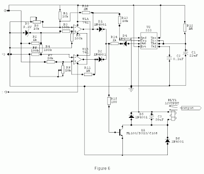
Under normal operating conditions i.e. when the input voltage is between maximum and minimum limit the output from the both the comparators are low. The transistor Q1 is OFF and the relay is in de-energized (pole connected to N/C pin) state and the output is obtained.
When the input voltage is below or above the limits set by the pre-sets R8 or R9, the output of the Op-Amps goes either low or high and diodes D1 or D2 would be forward biased depending on the situation. Transistor Q1 switches ON and the flow of current from collector to emitter energizes the relay and the output is cutoff.
A small amount of hystersis has been added via feed back resistors R10 & R11 so that the relay turns on when the level falls to a particular value but does not turn again until it raises a substantial amount above this value. Other wise the relay contacts will frequently turn on/off and produce chattering.
Construction Hints
1) I used a piece of varoboard, which has copper strips on one side to mount the components, and housed the entire circuit and the transformer in a discarded ATX PC power supply box.
1) I used a piece of varoboard, which has copper strips on one side to mount the components, and housed the entire circuit and the transformer in a discarded ATX PC power supply box.
2) An autotransformer has been used to set the limits. Set the output of the autotransformer to 250V AC and connect it to the primary of transformer T1 (see Figure 1). Then adjust the pre-set R9 such that relay just energizes. This is the high limit. Next set the output of the autotransformer to 200V AC and adjust the pre-set R8 such that the relay energizes. Please note that these are my preferred limits but you may select any range from say 170 to 270V AC.
3) A neon with a suitable resistor could be connected between the AC supply lines as an ON indicator. Alternatively, LED with a current limiting resistor could be connected between the relay coil so when the relay is energized LED will indicate the situation.


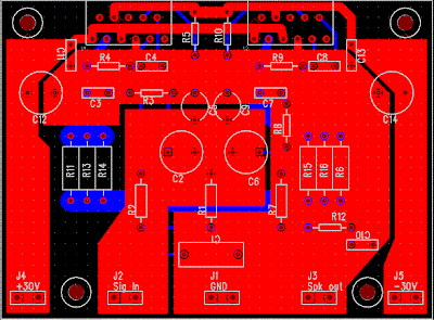
 The LM3886 circuit is in a non-inverted configuration, so the input impedance is determined by the input resistor R1, i.e. 47k. The 680 ohm and 470pF resistor capacitor filter network is used to filter out the high frequency noise at the RCA input. The 220pF C4 and C8 capacitors are used to shot out the high frequency noise at the LM3886 input pins.