Showing posts with label a. Show all posts

Friday, January 10, 2014

Up Down Timer For A Power Antenna

This up/down timer was designed to control a power antenna on a late-model vehicle. Normally, this vehicle uses a body computer to control the antenna. However, the person who owned the vehicle wanted to install his own high-powered audio stereo system. The original stereo system was tied in with the body computer and this meant that a separate antenna controller was required for the after-market sound system.

Also, the power antenna fitted did not have limit switches inside, hence the need for a timed control circuit. Heres how the circuit works. first, assume that the radio antenna control output is not switched on - ie, the radio is switched off. In that case, relay RLYC will be off and so relay RLYA will also be off, as is the motor. Conversely, when the radio is switched on, the radio antenna control output line switches to +12V.

And when that happens, RLYC closes its contacts and applies power to the circuit. As a result, C2 (330OF) quickly charges via D4, while Q4 is biased on via D5 and R5. This ensures that Q3 and relay RLYB remain off. At the same time, Q2 is is turned on, thus turning on RLYA and applying power to the motor. This drives the antenna in the up direction. During this time, C1 charges via R2.

Circuit diagram:

Up and down timer for a power antenna circuit schematic

When the voltage across the capacitor reaches +8.1V, Q1 turns on via ZD1 and so Q2 turns off and switches off the relay - ie, this gives the "up" timeout. Using the values shown for C1, R2 and ZD1 gives an "up" duration of approximately 6 seconds - long enough to fully extend the antenna. D1 discharges C1 (via resistor R1) when the +12V supply is later removed. When the radio is switched off (or a CD placed into the stereo unit), the radio antenna control output switches back to 0V.

This does several things: first, it turns Q4 off and this allows Q3 to turn on due to the stored charge in C2. Q3 and RLYB now turn on for about six seconds - ie, while C2 discharges via R4 - and this switches power to the motor in the opposite direction to drive the antenna down. Diodes D4 and D5 are there to prevent C2 from discharging back via the circuitry around on Q1 and Q2.

Author: Peter Howarth - Copyright: Silicon Chip Electronics
Read More..

Friday, December 27, 2013

Build a Pulse Charger for reviving tired Lead Acid batteries

If you own a motorcycle, a motor home, a caravan, a lawn mover, a day cruiser or maybe a vintage car you must at some point had to write off a lead acid battery. When a battery is improperly charged or allowed to self-discharge as occurs during non-use, sulphate crystals build up on the batterys plates. The sulphate preventing the battery from being fully charged and therefore it is unable to deliver its full capacity. When trying to charge a battery in this state it only gets hot and looses water, the gravity of the electrolyte is not increasing to its normal “full charge” state. 

 Pulse Charger for reviving tired Lead Acid batteries Circuit Diagram

Pulse Charger for reviving tired Lead Acid batteries


The only thing you do is killing the battery completely. If a battery has a resting voltage of at least 1.8 Volts/cell and no cells are shorted, desalination of its plates can be done. This circuit is an add-on and part for a modification of a normal charger and it takes care of the sulphate problem.

The project: get hold of an old charger, big or small it’s your choice depending on the size of batteries you normally handle (bigger is better). There are some tricks to boost the performance if you need it. Start by ripping out everything except the transformer and the rectifier. Some older chargers are equipped with fin rectifiers, which have high voltage drop and must be replaced. Replace with a rugged bridge rectifier that can cope with the amperes. All wiring on secondary should be short and heavy wire. The rectifier should be bolted to the chassis to keep cool. If the charger have a high/low switch it’s a bonus, if not you can in some cases add a few turns of wire on the secondary winding. 

The circuit; a 14-stage ripple counter and oscillator IC 4060 produce a pulse, which is the heartbeat of the circuit. The pulse is feed to the 555 timer that deicide the length of the active output. With the switch you can select long or short pulse output. The output of the 555 timer triggers the zero-cross opt isolator triac driver MOC 3041 via a transistor. This gives the charger transformer a soft start via the triac and the snubber circuit. A small power supply is necessary for the circuit and consists of T1 a transformer 15V 0.1A secondary, a bridge rectifier, a regulator and two caps. Because this project include a charger that is (X) the outcome can differ in performance from one case to another. However this do not mean that your project doesn’t work, but the efficiency can vary. Some notes the snubbercap is a high voltage AC type (X) and the resistors on the mains side is at least 0.5W type. Use a triac that can take 400V+ and 10A+, I use BTA 25.600 but this is overkill in most cases. No PCB sorry!

How it works:
Well the short version. The object is to get the cell voltage high enough for the sulphate to dissolve without boiling or melting the battery. This is achieved by applying higher voltage for shorter periods and let the battery rest for a while. The pulses on short range is about 0.5s on / 3s off and the long pulse range is 1.4s on / 2s off. These times can vary depending on component tolerances. Start on long pulse and if you discover “boiling” (more than with normal charging) in the electrolyte switch to short puls. Don’t leave the process unattended, at least until you know how your specific version of this project turns out. I built ver.1 of this circuit some 10 years ago and have experimented with it but I’m sure someone can improve it further.
Read More..

Wednesday, December 25, 2013

Build a Single cell Charger Circuit Diagram

This Single cell Charger Circuit Diagram detects a full-charge state and automatically switches to a float condition —from 240 mA to 12 mA. The circuit uses the 555 timer.


 Build a Single cell Charger Circuit Diagram


Build a Single cell Charger Circuit Diagram
 
Read More..

Friday, December 20, 2013

Build a High And Low Voltage Cut Off With Time Delay Circuit Diagrams

The power line fluctuations and cut-offs cause damages to electrical appliances connected to the line. It is more serious in the case of domestic appliances like fridge and air conditioners. If a fridge is operated on low voltage, excessive current flows through the motor, which heats up, and get damaged.

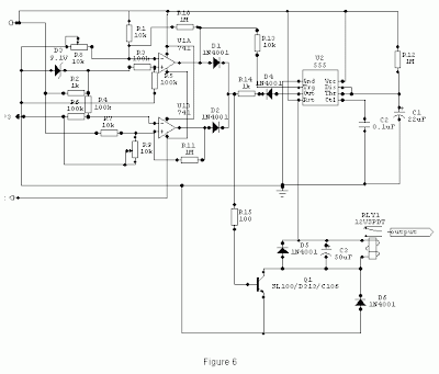
The under/over voltage protection circuit with time delay presented here is a low cost and reliable circuit for protecting such equipments from damages. Whenever the power line is switched on it gets connected to the appliance only after a delay of a fixed time. If there is hi/low fluctuations beyond sets limits the appliance get disconnected. The system tries to connect the power back after the specific time delay, the delay being counted from the time of disconnection. If the power down time (time for which the voltage is beyond limits) is less than the delay time, the power resumes after the delay: If it is equal or more, then the power resumes directly.

This circuit has been designed, built and evaluated by me to use as a protector for my home refrigerator. This is designed around readily available semi-conductor devices such as standard bipolar medium power NPN transistor (D313/SL100/C1061), an 8-pin type 741 op-amp and NE555 timer IC. Its salient feature is that no relay hunting is employed. This draw back is commonly found in the proctors available in the market.

The complete circuit is consisting of various stages. They are: - Dual rail power supply, Reference voltage source, Voltage comparators for hi/low cut offs, Time delay stage and Relay driver stage. Lets now look at the step-by-step design details.

Dual rail power supply.
This is a conventional type of power supply as shown in Figure 1. The power is applied through the step-down transformer (230/12-0-12V/500mA). The DC proportional to the charging input voltage is obtained from bridge rectifier. Two electrolytics are there to bypass any spikes present. Bridge is capable of handling currents up to 1 Amp.
Output is given by: -
V(out) = 0.71 X V (secondary)
= 0.71 X 24V
= 17.04 V
(This equation is similar for the negative rail as well)

Circuit diagram

Build a High And Low Voltage Cut Off With Time Delay


Low voltage cut off op-amp
Figure 2 shows the use of very common and easily available op-amp 741 as a comparator. The op-amp is available in TO-5 and DIP type packing.

Circuit diagram

Build a High And Low Voltage Cut Off With Time Delay2


In this ckt the zener diode D1 and it’s associated resistor R1 are connected to the non-inverting terminal (+ve) of 741 to give the suitable reference voltage. The DC voltage from the sensor is given to the inverting (-ve) terminal through pre-set R2.This is used to set the input level.
When the sensor input is less than Zener voltage the output from the Op-amp remains high and when it is greater than Zener voltage the output goes low. When the sensing voltage is equal to Zener voltage the output of the op-amp is approximately zero.
This phenomenon is used as a decision for switching the relay and to give cutoff in a low voltage situation.

High voltage cut off op-amp
Here the op-amp is used as a inverted amplifier. See Figure 3.Zener and resistor network gives reference voltage to the inverting terminal (-ve) of op-amp. Sensing voltage derived through the 10 K pre-set is given to the non- inverting (+ve) terminal and this sets the high level cut.

When the input DC from the sensor is less than Zener voltage the output of the op-amp is low and vice-versa. When the input DC voltage is equal to the zener voltage, the op-amps output is approximately zero.

Circuit diagram

Build a High And Low Voltage Cut Off With Time Delay3


Time delay
I’ve selected the 555 timer due to following reasons.
1. Timing from microseconds through hours.
2. Ability to operate from wide range of supply voltages.
3. High temperature stability.
4. Easily Available.
5. Its triggering circuit is quite sensitive.

This is basically a monostable. The external timing capacitor C2 is held initially discharged by the timer. The circuit triggers upon receiving a pulse to its pin 2 when the level reaches 1/3 Vcc. Once triggered., the circuit will remain in that state until the set time is elapsed or power to the circuit cuts off. The delayed period in seconds is 1.1 C2.R1 where R1 is in megohms and C2 is in microfarads. In practice, R1 should not exceed 20 M. If you use an electrolytic capacitor for C2, select a unit for low leakage. The time delay may have to be adjusted by varying R1 to compensate for the wide tolerance of electrolytics.

Circuit diagram

Build a High And Low Voltage Cut Off With Time Delay


Relay Driver
The output from the voltage level detectors cannot directly drive the relay and hence the relay driver is used.

Circuit diagram

Build a High And Low Voltage Cut Off With Time Delay5


In this a relay (12V <500 ohms) is connected to the collector of NPN transistor. The out put voltage from the comparator is applied to the base of NPN transistor through a resistance R1. When the output from the comparator is low the transistor is in OFF state and the relay is in de-energized state. Similarly when the output from the comparator goes high the transistor switches ON and the flow of current from the collector to emitter of transistor energizes the relay.

Generally in a relay driver circuit, parallel to the relay coil, a diode or a capacitor is used. This is to eliminate the back e.m.f generated by the relay coil when currents are suddenly broken. Capacitor C1 is connected in parallel to the coil, which filters out the back emf but it, slows down the working of relay.

A better method is to connect two diodes (as shown in the figure 5) that stop the relay – transistor junction swinging more than 600mV above the positive rail or below the zero-volt rail. During normal operation the diodes are reverse biased and have no effect on the performance of circuit. But when back emf is induced, the diodes conduct heavily and absorb all transient voltages. However, I have employed the both methods.
The Complete Circuit

Circuit diagram


Build a High And Low Voltage Cut Off With Time Delay1


Under normal operating conditions i.e. when the input voltage is between maximum and minimum limit the output from the both the comparators are low. The transistor Q1 is OFF and the relay is in de-energized (pole connected to N/C pin) state and the output is obtained.

When the input voltage is below or above the limits set by the pre-sets R8 or R9, the output of the Op-Amps goes either low or high and diodes D1 or D2 would be forward biased depending on the situation. Transistor Q1 switches ON and the flow of current from collector to emitter energizes the relay and the output is cutoff.

A small amount of hystersis has been added via feed back resistors R10 & R11 so that the relay turns on when the level falls to a particular value but does not turn again until it raises a substantial amount above this value. Other wise the relay contacts will frequently turn on/off and produce chattering.

Construction Hints
1) I used a piece of varoboard, which has copper strips on one side to mount the components, and housed the entire circuit and the transformer in a discarded ATX PC power supply box.

2) An autotransformer has been used to set the limits. Set the output of the autotransformer to 250V AC and connect it to the primary of transformer T1 (see Figure 1). Then adjust the pre-set R9 such that relay just energizes. This is the high limit. Next set the output of the autotransformer to 200V AC and adjust the pre-set R8 such that the relay energizes. Please note that these are my preferred limits but you may select any range from say 170 to 270V AC.

3) A neon with a suitable resistor could be connected between the AC supply lines as an ON indicator. Alternatively, LED with a current limiting resistor could be connected between the relay coil so when the relay is energized LED will indicate the situation.
Read More..

Tuesday, October 8, 2013

Dimmer With A MOSFET

This circuit shows that dimmers intended for use at mains voltage do not always have to contain a triac. Here, a MOSFET (BUZ41A, 500 V/4.5A) in a diode bridge is used to control the voltage across an incandescent bulb with pulse-width modulation (PWM). A useful PWM controller can be found elsewhere in this issue. The power supply voltage for driving the gate is supplied by the voltage across the MOSFET. D6, R5 and C2 form a rectifier. R5 limits the current pulses through D6 to about 1.5 A (as a consequence it is no longer a pure peak rectifier). The voltage across C2 is regulated to a maximum value of 10 V by R3, R4, C1 and D1. An optocoupler and resistor (R2) are used for driving the gate.

R1 is intended as protection for the LED in the optocoupler. R1 also functions as a normal current limiting device so that a ‘hard’ voltage can be applied safely. The optocoupler is anold acquaintance, the CNY65, which provides class-II isolation. This ensures the safety of the regulator. The transistor in the optocoupler is connected to the positive power supply so that T1 can be brought into conduction as quickly as possible. In order to reduce switching spikes as a consequence of parasitic inductance, the value of R2 has been selected to be not too low: 22 kΩ is a compromise between inductive voltages and switching loss when going into and out of conduction.

Dimmer With A MOSFET circuit schematic

An additional effect is that T1 will conduct a little longer than what may be expected from the PWM signal only. When the voltage across T1 reduces, the voltage across D1 remains equal to 10 V up to a duty cycle of 88 %. A higher duty cycle results in a lower voltage. At 94 % the voltage of 4.8 V proved to be just enough to cause T1 to conduct sufficiently. This value may be considered the maximum duty cycle. At this value the transistor is just about 100 % in conduction. At 230 V mains voltage, the voltage across the lamp is only 2.5 V lower, measured with a 100-W lamp. Just to be clear, note that this circuit cannot be used to control inductive loads. T1 is switched asynchronously with the mains frequency and this can cause DC current to flow.

Electronic lamps, such as the PL types, cannot be dimmed with this circuit either. These lamps use a rectifier and internally they actually operate off DC.A few remarks about the size of R3 and R4. This is a compromise between the lowest possible current consumption (when the lamp is off) and the highest possible duty cycle that is allowed. When the duty cycle is zero, the voltage across the resistors is at maximum, around 128 V with a mains voltage of 230 V. Because (depending on the actual resistor) the voltage rating of the resistor may be less than 300 V, two resistors are connected in series. The power that each resistor dissipates amounts to a maximum of 0.5W. With an eye on the life expectancy, it would be wise to use two 1-W rated resistors here.
Read More..

Friday, September 27, 2013

A 12V Car Charger For ASUS Eee Notebook

The ASUS Eee is a fantastic ultra-portable notebook with almost everything required for geeks (and nothing that isn’t). Plus it features fantastic build quality and is very well priced. If you live in New Zealand you can get them from DSE; at the time of writing they are the exclusive supplier. I worked out it’s the same cost as importing one once you include all the duties and tax, plus you get the advantage of a proper NZ-style mains charger. Anyway, being so small I thought it would be nice to be able to carry this around in the car. Unfortunately I couldn’t find a car charger available anywhere at the time so I decided to tackle the problem myself. As a bonus this provides an opportunity for an external high-capacity battery.
asus eee 701
Commercial Equivalent:
I thought at this stage it would be worth noting that a commercial car charger is now available for less than it cost me to build this from Expansys and is available in most countries (select your location on their site). It outputs 9.5v from 10-18v in at up to 2.5A. I’d actually recommend it over the design here is it seems to perform better at lower voltages (that one works down to 10V). However I have kept this page up as a reference for those who enjoy tinkering.
Design:
The charger included with the Eee is rated at 9.5v, 2.315A. There isn’t a fixed voltage regulator available for this exact voltage, so the circuit needed to be designed around an adjustable regulator. I decided to design the charger around the LM2576 “Simple Switcher” IC from National Semiconductor. There are tons of ICs like this available, many of which are a bit more efficient, however I selected this one because it is readily available and relatively cheap. It also has a lower drop-out voltage (~2V) than many other chips I looked at which is important when powering the device from a car or 12v SLA battery.
eee_car_charger_circuit d
This circuit could have used a standard three pin regulator IC such as the LM317, however most types require an external transistor when handling so much current and not to mention the fact that they are very inefficient; they draw the same amount of current from the input as the load and the difference in power is dissipated as heat. The main problem with using the LM2576 is the fact it needs quite a large inductor due to its somewhat low switching frequency. The inductor I used is made by Pulse Engineering, part number PE92108KNL. I’d prefer a smaller one, however I couldn’t find one capable of supplying the required current that I could purchase in single units. Besides the PE92108KNL is apparently designed specifically to work with the LM257x series.
charger_case_opens
The circuit also includes a low voltage cut-out based on a 9.1v Zener diode and BC337 transistor that will shut down the regulator if the input voltage is below 11.5V. This prevents unstable operation of the regulator at lower input voltages, and also helps prevent accidental flattening of the supply battery. Substituting this transistor for similar type may affect the cut-out voltage; the Vbe of the transistor should be 1.2v.All of the components used should be pretty readily available in most areas. I got everything from Farnell. Jaycar also sells everything except the inductor. Make sure you specify high temperature, low ESR capacitors as these help result in more stable operation and better efficiency of the charger.
eee_car_charger_schematic_monow
Unfortunately the end result is a charger that is slightly bulkier than I would really like. I attempted to fit this inside an old mobile phone charger case so the whole thing could hang out of the cigarette lighter, however I ran into trouble making the circuit stable enough and dissipating all the heat. Due to the high current involved compared to a mobile phone charger the components are much bulkier so it’s pretty tricky to get all to fit! If I do get it finished I’ll add an update.
Parts List:
  • 2x 10k resistor (R1 & R4)
  • 2x 22k resistor (R2 & R3)
  • 1x 1.5k resistor (R5)
  • 1x 120μF 25v electrolytic capacitor (C1)
  • 1x 2200μF 16v electrolytic capacitor (C2)
  • 1x 1N5822 Schottky diode (or equivalent)
  • 1x 9.1v 0.5W Zener diode
  • 1x BC337 NPN transistor
  • 1x LM2576T-ADJ IC
  • 1x 100uH, 3A inductor (e.g. Pulse PE92108KNL)
  • 25°C/W or better minature heatsink (e.g. Thermalloy 6073)
  • Cigarette lighter plug with 3A fuse and 2.1mm DC plug (e.g. DSE P1692)
  • 2.1mm DC chassis mount socket
  • 1.7mm x 4.75mm (ID x OD) DC plug and cable
  • Small plastic enclosure
Building It:
Make yourself a PCB using the template below (600dpi). I simply laser print (or photocopy) the design onto OHP transparency sheet and then transfer the toner onto a blank PCB using a standard clothes iron. Any missing spots can be touched up with a permanent marker before etching. This is quick, usually results in pretty tidy boards and hardly costs a thing. There is a tutorial on a variation of this method at http://max8888.orcon.net.nz/pcbs.htm.
eee_car_charger_pcbs
Install the components on the PCB and triple check the layout before soldering. It is much easier to start with the low profile components such as resistors and diodes, then install the larger components after-wards. Don’t forget the wire link; this is shows as a red line on the layout guide above. Remember to smear a small amount of heatsink compound on the regulator tab before mounting the heatsink.
eee_car_charger_pcb_layoute
For a case I used a small plastic enclosure from DSE, part H2840, as it was all the local store had in stock that was remotely suitable. The PCB is designed to fit into this particular case, however any small box should be suitable. If you have a dead laptop charger lying about it might be worth ripping the guts out of that and salvaging the case. If your enclosure is different you may need to modify the design to suit, so I have provided the schematic and PCB design files for download. They were created using Eagle. The Eee uses a standard 1.7mm DC power connector with a positive tip.
eee_car_chargerw1
Testing:
Connect the circuit to a 12v supply. If you use a car or lead acid battery ensure you have a 3A fuse fitted in line with the circuit before connecting it, just in case. Use your multimeter to check that the circuit outputs about 9.45v with no load. Connect a 12V, 21W lamp (e.g. old brake lamp from a car) or similar load across the output and check that the voltage doesn’t vary much. You should now be able to connect your Eee. The circuit design should be good for up to 2.5A, so there is plenty of margin for the Eee to fully function and charge its own battery off this supply.
     eee_external_battery0
SLA Battery Carry-bag:
Jaycar have a really cool carry bag with a shoulder strap designed to perfectly fit a 12v 7AH sealed lead acid battery. The bag features a fused cigarette lighter socket and is the perfect compliment to this charger. It works well with the Eee and provides hours of extra use. The shoulder strap means it’s not too bothersome to carry about and the charger circuit itself zips up neatly inside the bag. The under-voltage cut-off means the battery will never run completely flat, and the Eee will simply cut over to its internal battery once the SLA runs out. I got my SLA battery from Rexel as they are much cheaper (approx NZ$18 including GST last time I bought one) and they don’t sit as long on the shelf as many other suppliers.
inside_bag-charger l
Disclaimer:
This circuit is intended for people who have had experience in constructing electronic projects before. The circuit design and build process are provided simply as a reference for other people to use and I take no responsibility for how they are used. If you proceed with building and/or using this design you do so entirely at your own risk. You are free to use the content on this page as you wish, however I do ask that you include a link or reference back to this page if you distribute or publish any of the content to others.
Read More..

Thursday, September 12, 2013

Lock Down USB Ports via a PIC Based Smart Card Reader

What i am making here is a USB lock with smartcard key. The idea is that a phonecard reader made with a PIC micro will be able to store a number of different phonecards into memory. Whenever one of these cards is inserted into the slot, it will activate a 4-ports USB On/Off switch. If the card is removed, the USB ports will be de-activated.

Lock Down USB Ports via a PIC-Based Smart Card Reader
Read More..

Wednesday, September 11, 2013

Hg Lamp to a Powerful UV Light Source

I got myself some UV-curable solder mask for my PCB workshop, and as soon as i got it, i discovered that my UV artwork transfer box is totally incapable to activate the UV paint and cure it. I began searching the net for powerful UV lamps, and then it hit me: Some months ago i uploaded a theory regarding the Cold and Hot cathode discharge lamps. During my research for these lamps i found out that they can provide directly visible light (lamps without internal coating), or they produce UV radiation. The lamps that produce UV radiation have an extra coating on their internal surface which glows when excited by the UV rays, thus producing light!

Hacking a Hg Lamp to a Powerful UV Light Source
Read More..

Sunday, April 21, 2013

A Simple Function Generator

Simple triangle-wave generators have a weak point in that the waveform of their output signal normally cannot be modified. The circuit presented here makes it possible to easyly alter the waveform of a linearly rising and steeply trailing saw-tooth sign via a symmetrical triangle-wave to a slowly trailing, steeply rising linear sawtooth. The wanted waveform could additionally be selected impartially of the frequency, which can additionally be varied uniformly from zero.2 Hz to eight kHz. At the same time, an oblong signal with variable responsibility cycle (also unbiased of frequency) is on hand at the rectangular-signal output of the circuit.

Simple_Function_Generator_Circuit_Diagram1 
The circuit consists of integrator IC1b, whose output is applied to comparator IC1c. The output of the comparator is a rectangular signal The output of IC1b is raised through amplifier IC1d to a level that enables the full output voltage vary of the operational amplifier for use. Op amp IC1a provides a secure virtual earth, whose stage is set to 1 of 2 the availability voltage with P1. The easy surroundings of the frequency is made that which you can imagine by means of comments of part of the output of the comparator to the input of the integrator by approach of P2. This preset is regularly now not equipped in usual triangle-wave turbines. Network D1-R1-D2-R2-P3 makes it possible to provide integrator capacitor C3 completely different charging and discharge times.

This association enables the output sign at A1 and the accountability cycle of the rectangular wave signal at A2 to be various. Varying the amplification factor with P5 has no impact on the frequency set with P2. The slope of the signal aspects, the transient responses, and the output voltage range (rail-to-rail or with some voltage drop) depend upon the variety of op amp used. The TL084 used in the prototype offers a just right compromise between worth and assembly the wanted parameters. The circuit is highest constructed on a small piece of prototyping board. The circuit draws a present of no longer more than 12 mA.

Brief parameters:
Provides triangle-wave, sawtooth or rectangular signal
Waveform variable impartially of frequency (triangle wave and sawtooth)
Duty cycle of rectangular sign will be set independently of frequency
Applications:
Test and dimension
Pulse-width control
Summary of preset action:
P1 – units digital earth to a degree equal to Ucc/2;
P2 – units the frequency;
P3– units the waveform;
P4 – units the hysteresis of the comparator (frequency and amplitude of the triangle-wave sign)
P5 – sets the amplification of the triangle-wave and sawtooth alerts.
Read More..

Wednesday, April 10, 2013

A Car Battery Monitor

A close call on the road can really focus your mind on the importance of having a battery monitor in a car. I had been enjoying a pleasant week of travelling around the countryside at a leisurely pace and taking in the beautiful scenery each day. It wasnt until the final day, with the big rush to return home, that I had to drive at night.My home is deep in the country and on the road I was travelling the closest petrol station may be 80km away. I was travelling through an area that is full of open-cut coal mines and large heavily loaded semi-trailers constantly pound the roads, travelling at quite high speeds. It was around 8pm at night and everything was very dark no street lights or house lights anywhere.

Just as I was going up a hill, the lights began to dim and the engine coughed. A large semi-trailer loomed in the rear-vision mirror as I pushed the clutch in and tried to restart. My speed was falling rapidly and my lights were blacked out - I was like a sitting duck in the middle of the road, as the semi-trailer came rapidly bearing down on me. I just managed to pull the car off the road, as the semi-trailer came screaming past, missing me by inches! After calling for assistance from the NRMA, the problem was found to be a fault in the alternator, which was failing to charge the battery. The battery voltage had been falling under the heavy load of the lights and at the worst possible time, there was not sufficient power for the lights or the motor.

After the initial shock wore off, I put on my thinking cap to come up with a PIC-based solution to the problem. What was really needed was a display and a buzzer, to get my attention should the voltage fall outside a specified range. So my design criteria was set, a series of LEDs could indicate the voltage and a buzzer would also be used to warn of problems.
Main Features:
  • Visual indication of battery voltage
  • Audible warning when voltage becomes low
  • Screw terminals for easy connection
  • Simple and easy to build
Circuit details:

The circuit is based on PIC16F819 18-pin microcontroller which has an analog-to-digital (A/D) input to monitor the battery voltage and outputs capable of driving LEDs directly, to keep the component count down. There are seven LEDs in all, giving a good range of voltage indication. The topmost LED, LED1, comes on for voltages above 14V which will occur when the battery is fully charged. LED2 indicates for voltages between 13.5V and 14V while LED3 indicates between 13V and 13.5V. Normally, one of these LEDs will be on. LED4 covers 12.5V to 13V while LED5 covers 12V to 12.5V. LED6 covers from 11.5V to 12V while LED7 comes on for voltages below 11.5V. These two LEDs are backed up by the piezo chime which beeps for voltages between 11.5V and 12V and becomes more insistent for voltages below 11.5V.

That might seem fairly conservative. After all, most cars will start with no troubles, even though the battery voltage might be a touch below 12V, wont they? Well, no. Some modern cars will happily crank the motor at voltages below 11V but their engine management will not let the motor start unless the voltage is above 11V. So dont think that a modern car will always start reliably. This little battery monitor could easily prevent a very inconvenient failure to start! So lets describe the rest of the circuit. The incoming supply is connected via diode D1 which provides protection against reverse polarity while zener diode ZD1 provides protection from spike voltages.

A standard 7805 3-terminal regulator is then used to provide a stable 5V to the microcontroller. The battery voltage is sensed via a voltage divider using 33kΩ and 100kΩ resistors. This brings the voltage down to within the 0-5V range for the A/D input of the PIC16F819. Port B (RB0 to RB7) of the microcontroller is then used to drive the various LEDs, with current limiting provided via the 330Ω resistor network. RB7, pin 13, drives a switching transistor for the piezo buzzer.

Software:
For the software, the design follows the basic template for a PIC microcontroller. Port A and its ADC (analog-to-digital converter) function are set up while port B functions as the output for the LEDs and buzzer. Once the set-up is complete, a reading will be taken at port RA2, the input for the A/D convertor. This reading is then compared with a series of values to determine the range of the voltage. This is similar to a series of "if" statements in Basic language. If the voltage is found to be within a certain range, the relevant port B pin will be turned on. If the voltage is below 12V, the buzzer will be turned on for a brief period, to signal a low battery condition. As the voltage falls below 11.5V, the frequency of the beeps will increase, to signal increased urgency.
Building it:

All the parts are mounted on a small PC board measuring 46 x 46mm (available from Futurlec). The starting point should be the IC socket for the PIC16F819, as this is easiest to mount while the board is bare. The next item can be the PC terminal block. The resistors and capacitors can then follow. Make sure the electrolytics are inserted with correct polarity.

Make sure that you do not confuse the zener (ZD1) with the diode when you are installing them; the diode is the larger package of the two.
Even more important, dont get the 78L05 3-terminal regulator and the 2N3906 transistor mixed up; they come in identical packages. The 78L05 will be labelled as such while the 2N3906 will be labelled "3906". And make sure you insert them the correct way around. The buzzer must also be installed with the correct polarity. The 330Ω current limiting resistors are all in a 10-pin in-line package. There are four green LEDs, two yellow and one red. They need to be installed in line and with the correct orientation.
Testing:
Before you insert the PIC16F819 microcontroller, do a voltage check. Connect a 12V source and check for the presence of 5V between pins 14 & 5 OF IC1. If 5V is not present, check the polarity of regulator REG1 and the polarity of the diode D1. If these tests are OK, insert the IC and test the unit over a range of voltage between 9V and 15V. Make sure that all LEDs come on in sequence and the piezo buzzer beeps for voltages below 12V.
Now it is matter of installing the unit in your car. It is preferable to install the unit in a visible position for the driver. However, it should not obscure any other instruments. The unit should be connected to the cars 12V supply after the ignition switch. This will turn the unit off with the other instruments and prevent battery drain while the motor is not running.
Read More..