Showing posts with label with. Show all posts

Friday, December 20, 2013

Build a High And Low Voltage Cut Off With Time Delay Circuit Diagrams

The power line fluctuations and cut-offs cause damages to electrical appliances connected to the line. It is more serious in the case of domestic appliances like fridge and air conditioners. If a fridge is operated on low voltage, excessive current flows through the motor, which heats up, and get damaged.

The under/over voltage protection circuit with time delay presented here is a low cost and reliable circuit for protecting such equipments from damages. Whenever the power line is switched on it gets connected to the appliance only after a delay of a fixed time. If there is hi/low fluctuations beyond sets limits the appliance get disconnected. The system tries to connect the power back after the specific time delay, the delay being counted from the time of disconnection. If the power down time (time for which the voltage is beyond limits) is less than the delay time, the power resumes after the delay: If it is equal or more, then the power resumes directly.

This circuit has been designed, built and evaluated by me to use as a protector for my home refrigerator. This is designed around readily available semi-conductor devices such as standard bipolar medium power NPN transistor (D313/SL100/C1061), an 8-pin type 741 op-amp and NE555 timer IC. Its salient feature is that no relay hunting is employed. This draw back is commonly found in the proctors available in the market.

The complete circuit is consisting of various stages. They are: - Dual rail power supply, Reference voltage source, Voltage comparators for hi/low cut offs, Time delay stage and Relay driver stage. Lets now look at the step-by-step design details.

Dual rail power supply.
This is a conventional type of power supply as shown in Figure 1. The power is applied through the step-down transformer (230/12-0-12V/500mA). The DC proportional to the charging input voltage is obtained from bridge rectifier. Two electrolytics are there to bypass any spikes present. Bridge is capable of handling currents up to 1 Amp.
Output is given by: -
V(out) = 0.71 X V (secondary)
= 0.71 X 24V
= 17.04 V
(This equation is similar for the negative rail as well)

Circuit diagram

Build a High And Low Voltage Cut Off With Time Delay


Low voltage cut off op-amp
Figure 2 shows the use of very common and easily available op-amp 741 as a comparator. The op-amp is available in TO-5 and DIP type packing.

Circuit diagram

Build a High And Low Voltage Cut Off With Time Delay2


In this ckt the zener diode D1 and it’s associated resistor R1 are connected to the non-inverting terminal (+ve) of 741 to give the suitable reference voltage. The DC voltage from the sensor is given to the inverting (-ve) terminal through pre-set R2.This is used to set the input level.
When the sensor input is less than Zener voltage the output from the Op-amp remains high and when it is greater than Zener voltage the output goes low. When the sensing voltage is equal to Zener voltage the output of the op-amp is approximately zero.
This phenomenon is used as a decision for switching the relay and to give cutoff in a low voltage situation.

High voltage cut off op-amp
Here the op-amp is used as a inverted amplifier. See Figure 3.Zener and resistor network gives reference voltage to the inverting terminal (-ve) of op-amp. Sensing voltage derived through the 10 K pre-set is given to the non- inverting (+ve) terminal and this sets the high level cut.

When the input DC from the sensor is less than Zener voltage the output of the op-amp is low and vice-versa. When the input DC voltage is equal to the zener voltage, the op-amps output is approximately zero.

Circuit diagram

Build a High And Low Voltage Cut Off With Time Delay3


Time delay
I’ve selected the 555 timer due to following reasons.
1. Timing from microseconds through hours.
2. Ability to operate from wide range of supply voltages.
3. High temperature stability.
4. Easily Available.
5. Its triggering circuit is quite sensitive.

This is basically a monostable. The external timing capacitor C2 is held initially discharged by the timer. The circuit triggers upon receiving a pulse to its pin 2 when the level reaches 1/3 Vcc. Once triggered., the circuit will remain in that state until the set time is elapsed or power to the circuit cuts off. The delayed period in seconds is 1.1 C2.R1 where R1 is in megohms and C2 is in microfarads. In practice, R1 should not exceed 20 M. If you use an electrolytic capacitor for C2, select a unit for low leakage. The time delay may have to be adjusted by varying R1 to compensate for the wide tolerance of electrolytics.

Circuit diagram

Build a High And Low Voltage Cut Off With Time Delay


Relay Driver
The output from the voltage level detectors cannot directly drive the relay and hence the relay driver is used.

Circuit diagram

Build a High And Low Voltage Cut Off With Time Delay5


In this a relay (12V <500 ohms) is connected to the collector of NPN transistor. The out put voltage from the comparator is applied to the base of NPN transistor through a resistance R1. When the output from the comparator is low the transistor is in OFF state and the relay is in de-energized state. Similarly when the output from the comparator goes high the transistor switches ON and the flow of current from the collector to emitter of transistor energizes the relay.

Generally in a relay driver circuit, parallel to the relay coil, a diode or a capacitor is used. This is to eliminate the back e.m.f generated by the relay coil when currents are suddenly broken. Capacitor C1 is connected in parallel to the coil, which filters out the back emf but it, slows down the working of relay.

A better method is to connect two diodes (as shown in the figure 5) that stop the relay – transistor junction swinging more than 600mV above the positive rail or below the zero-volt rail. During normal operation the diodes are reverse biased and have no effect on the performance of circuit. But when back emf is induced, the diodes conduct heavily and absorb all transient voltages. However, I have employed the both methods.
The Complete Circuit

Circuit diagram
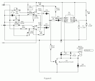

Build a High And Low Voltage Cut Off With Time Delay1


Under normal operating conditions i.e. when the input voltage is between maximum and minimum limit the output from the both the comparators are low. The transistor Q1 is OFF and the relay is in de-energized (pole connected to N/C pin) state and the output is obtained.

When the input voltage is below or above the limits set by the pre-sets R8 or R9, the output of the Op-Amps goes either low or high and diodes D1 or D2 would be forward biased depending on the situation. Transistor Q1 switches ON and the flow of current from collector to emitter energizes the relay and the output is cutoff.

A small amount of hystersis has been added via feed back resistors R10 & R11 so that the relay turns on when the level falls to a particular value but does not turn again until it raises a substantial amount above this value. Other wise the relay contacts will frequently turn on/off and produce chattering.

Construction Hints
1) I used a piece of varoboard, which has copper strips on one side to mount the components, and housed the entire circuit and the transformer in a discarded ATX PC power supply box.

2) An autotransformer has been used to set the limits. Set the output of the autotransformer to 250V AC and connect it to the primary of transformer T1 (see Figure 1). Then adjust the pre-set R9 such that relay just energizes. This is the high limit. Next set the output of the autotransformer to 200V AC and adjust the pre-set R8 such that the relay energizes. Please note that these are my preferred limits but you may select any range from say 170 to 270V AC.

3) A neon with a suitable resistor could be connected between the AC supply lines as an ON indicator. Alternatively, LED with a current limiting resistor could be connected between the relay coil so when the relay is energized LED will indicate the situation.
Read More..

Tuesday, October 8, 2013

Dimmer With A MOSFET

This circuit shows that dimmers intended for use at mains voltage do not always have to contain a triac. Here, a MOSFET (BUZ41A, 500 V/4.5A) in a diode bridge is used to control the voltage across an incandescent bulb with pulse-width modulation (PWM). A useful PWM controller can be found elsewhere in this issue. The power supply voltage for driving the gate is supplied by the voltage across the MOSFET. D6, R5 and C2 form a rectifier. R5 limits the current pulses through D6 to about 1.5 A (as a consequence it is no longer a pure peak rectifier). The voltage across C2 is regulated to a maximum value of 10 V by R3, R4, C1 and D1. An optocoupler and resistor (R2) are used for driving the gate.

R1 is intended as protection for the LED in the optocoupler. R1 also functions as a normal current limiting device so that a ‘hard’ voltage can be applied safely. The optocoupler is anold acquaintance, the CNY65, which provides class-II isolation. This ensures the safety of the regulator. The transistor in the optocoupler is connected to the positive power supply so that T1 can be brought into conduction as quickly as possible. In order to reduce switching spikes as a consequence of parasitic inductance, the value of R2 has been selected to be not too low: 22 kΩ is a compromise between inductive voltages and switching loss when going into and out of conduction.

Dimmer With A MOSFET circuit schematic

An additional effect is that T1 will conduct a little longer than what may be expected from the PWM signal only. When the voltage across T1 reduces, the voltage across D1 remains equal to 10 V up to a duty cycle of 88 %. A higher duty cycle results in a lower voltage. At 94 % the voltage of 4.8 V proved to be just enough to cause T1 to conduct sufficiently. This value may be considered the maximum duty cycle. At this value the transistor is just about 100 % in conduction. At 230 V mains voltage, the voltage across the lamp is only 2.5 V lower, measured with a 100-W lamp. Just to be clear, note that this circuit cannot be used to control inductive loads. T1 is switched asynchronously with the mains frequency and this can cause DC current to flow.

Electronic lamps, such as the PL types, cannot be dimmed with this circuit either. These lamps use a rectifier and internally they actually operate off DC.A few remarks about the size of R3 and R4. This is a compromise between the lowest possible current consumption (when the lamp is off) and the highest possible duty cycle that is allowed. When the duty cycle is zero, the voltage across the resistors is at maximum, around 128 V with a mains voltage of 230 V. Because (depending on the actual resistor) the voltage rating of the resistor may be less than 300 V, two resistors are connected in series. The power that each resistor dissipates amounts to a maximum of 0.5W. With an eye on the life expectancy, it would be wise to use two 1-W rated resistors here.
Read More..

Tuesday, September 3, 2013

Phone Hold With Music Circuit

Circuit Diagram 

Description
This circuit will allow you to place a phone call on hold and if you wish to have them listen to music while they are on hold. The circuit operates as follows: The RED wire from the phone jack is typically positive and the GREEN wire is negative or ground. When you want to place a call on hold, close S1 and hang up the handset. The resistor R1 simulates another phone off hook and allows enough
current to pass through to prevent the phone company from disconnecting the call. The resistor R2 and LED provide a visual indication that you have someone on hold ( this is optional )
The capacitor C1 and the transformer provide the interface to a radio or CD player headphone jack. Before you hook up the project to the phone line you must determine the polarity of the line. Place a voltmeter across the red and green wires of the telephone line, there should be about 48 volts
DC positive when the black lead of your meter is connected to the green phone wire. If it is negative 48 volts then reverse the wires.

Source -http://www.electronics-lab.com/
Read More..

Friday, April 12, 2013

Simple Tone Control Circuit with LM301A

This circuit and a simple collection circuit Tone Control. This circuit tone control with surgical Amp LM301A. The JFET 2N3684 feature gives a high input impedance and low noise for UN buffer zone opinion operational amplifier operated EQ sort. Could you see intimately of the circuit following hence as under.


Read More..

Thursday, April 11, 2013

Subwoofer amplifier with 30W output power

hifi amplifier
Amplifier circuit is very suitable for use in subwoofer amplifier system based on IC SI1030G. Amplfier has 30W output with 8 ohm impedance. Supply voltage required minimum of 12 volts and a maximum of up to 22 volts DC.

subwoofer audio amplifier with SI1030DL
Component List :
R1 = 100K
R2 = 1R
C1 = 2.2uF
C2 = 100uF
C3 = 47uF
C4 = 100nF
C5 = 10uF
C6 = 47uF
C7 = 100uF
IC = SI1020GL , SI1030G
Read More..

Flash Lights with HT2014L

Flash Lights with HT2014L


This scheme is almost the same with a flash light with LM3909. In this scheme only requires IC HT2014L as a leader, and a resistor and LED. For voltage here need ration power around 4.5 V. You can apply this series to a wider scale in comparing the use IC LM3909. For the scheme are below:


flash lights circuit
Read More..

Sunday, April 7, 2013

Simple Inverter with Two Transistors

The series below is a simple inverter circuit that will change the voltage of 12v dc to 220v ac, with use drive transistor 32 as its tip.
Inverter circuit is very simple and easy to assemble and is perfect for just starting to learn to assemble electronic circuits, you can use the transformer 2A to produce about 20 watts output. Do not forget to install coolers in its transistors. good luck.
Simple Inverter with Two Transistors

Read More..

Friday, April 5, 2013

50W audio amplifier with ICs

50W amplifier circuitschematic
The above amplifier circuit based on IC is STK075G, and another equation that is STK084G, STK085, STK086G. and among ic I mentioned that I recommend using ic high supply voltage and high output power and good quality. You can see every ic datasheet at Alldatasheet.com above. Supply voltage between 20 to 55 Volt DC.
Part List
R1 = 1K
R2 = 100R
R3 = 100R
R4 = 4.7R
R5 = 56K
R6 = 47R
C1 = 1uF
C2 = 470pF
C3 = 100uF
C4 = 100uF
C5 = 1800pF
C6 = 1uF
C7 = 1800pF
C8 = 0.047uF
C9 = 100uF
U1 = STK075G,  STK084G, STK085, STK086G
Read More..

Thursday, April 4, 2013

How to Calculate and Match an Inverter Circuit with Battery and Transformer

Making an inverter all by you can be definitely lot of fun. However if the results are not satisfactory can completely spoil the whole purpose of the project. Installing and configuring the various inverter parameter like the battery and the transformer to with the actual assembled circuit needs special care and attention for deriving optimal results from the assembly. The article broadly discusses how to calculate and match a battery and transformer wit the relevant circuit and also enlightens regarding the possible faults that might be encountered and the respective troubleshooting procedures.
The article enlightens the many newcomers with some of the important clues, which might be helpful while configuring an inverter circuit with the battery and the transformer, so that efficient and optimal results can be achieved.

Configuring Inverter Parameters

While making an inverter, two points must be broadly taken into account – the transformer must be rated twice the maximum load that is expected to be used with the inverter and the battery must be rated at 1/4 more than the transformer ratings.

For example, if the inverter is expected to work at 12 volts, with maximum loads of 200 watts, the transformer must be rated at least 500 watts, corresponding to 40 plus amperage, roughly (dividing 500 by 12), and the battery in turn must be rated at = ¼ multiplied by 40 = 10, therefore 40 + 10 = 50 AH (minimum).

After procuring all the necessary components as explained above, it would be important to get them checked for compatibility with one another.

Only the battery, which is one the most crucial member, hopefully will not require any prior checking, because the printed rating and the charged voltage conditions should be sufficient to prove its reliability. It is assumed here that the condition of the battery is good and it’s relatively new and “healthy.”

Next comes the transformer, which is another most important component of the inverter, surely needs a thorough technical assessment. It may be done as follows:


The rating of the transformer can be best checked in the reverse order, i.e. by connecting its higher voltage winding to the AC mains input and checking the opposite winding for the specified outputs.

If the current ratings of the lower voltage section are within the maximum limits of a regular multi-tester (DMM), then it may be checked by switching ON the above AC and connecting the meter (set at, say AC 20 Amp) across the relevant winding.


Hold the meter prods connected across the winding terminals for a couple of seconds to get the readings directly on the meter.

If the reading matches with the specified transformer current, or at least is close to it, means your transformer is OK. Lower readings would mean a bad or a wrongly rated transformer winding.

The assembled circuit broadly needs to be checked for proper oscillation outputs across the bases of the power transistors or the mosfets.

This may be done by connecting the circuit to the battery, but without including the transformer initially. The checking should be done using some good frequency meter or if possible using an oscilloscope.
If the above gadgets are not there with you, a crude testing can be performed using a pair of ordinary headphones. Connect the headphone jack to the bases of the relevant power transistors; you should get a strong humming sound in the headphones, confirming a sound functioning of the oscillator stages.

The above confirmations should be enough to prompt you to configure all the sections together.

Connect the transformer to the relevant transistor or the power devices terminals; make sure the power devices are correctly integrated with the oscillator stage.

Finally the battery may be connected to the power inputs of the above configuration, again do not forget to include an appropriately rated FUSE in series with the battery positive.

The output of the transformer now may be attached with the specified maximum load and the power may be switched ON.

If everything’s is wired up correctly, the load should start operating at its full fledged power, if not, then something’s wrong with the circuit stage.

Since the oscillator section was appropriately checked before the final installations, surely the fault may lie with the power device stage.


If the fault is associated with low power outputs, the base resistors may be tweaked for possible faults, or may be reduced by adding parallel resistors to their existing base resistors.


The results may be checked as discussed above, if the results are positive and if you find improvements in the power outputs, the resistors may be further modified as desired, until the expected power output is delivered.


However this may lead to further heating of the devices and due care must be observed to keep them under check by either including cooling fans or increasing the heatsink dimensions.


However if the fault is accompanied with blowing of the fuse would mean a definite short circuit somewhere in the power stage.

The problem may also indicate a wrongly connected power device, a blown-of power device due to a possible shorting between the power device’s output terminals or the any of the terminals that needs to be perfectly kept aloof of each other.

Having explained a few of the above possibilities while configuring an inverter optimally, a thorough knowledge regarding electronic becomes an absolute necessity from the part of the individual who may be involved with the construction, without which the proceeding with the project may somehow get jeopardized.
Read More..

Tuesday, April 2, 2013

Fuse Circuit with Status Indicator

This is a design circuit diagram of a fuse circuit. The circuit has an automatic status indicator. This circuit can be added to circuit that operates from 12V DC. As long as the fuse is intact, the LED D3 will glow continuously and when the fuse blows off the LED will start and continue blinking. The fuse F1 can be a metal wire fuse with your required rating. This is the figure of the circuit.


The operation of the circuit is begin from the first part of the circuit that includes an astable multi vibrator built around transistors Q1 and Q2.The output of the multi vibrator is coupled to the base of Q3 via diode D2.When the fuse is intact the base of Q3 will be pulled to a positive voltage by the resistor R5. The transistor will be ON and the LED D3 remains glowing. When the fuse of blown off, the base of Q3 will no longer be pulled to positive voltage and now the only biasing available at the base of Q3 will be the output from the astable multi vibrator. Now the transistor Q3 will start switching in the frequency of astable multi vibrator and the LED will blink in accordance.

Read More..