Showing posts with label circuit. Show all posts

Wednesday, December 25, 2013

Build a Single cell Charger Circuit Diagram

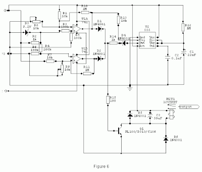
This Single cell Charger Circuit Diagram detects a full-charge state and automatically switches to a float condition —from 240 mA to 12 mA. The circuit uses the 555 timer.


 Build a Single cell Charger Circuit Diagram


Build a Single cell Charger Circuit Diagram
 
Read More..

Friday, December 20, 2013

Build a High And Low Voltage Cut Off With Time Delay Circuit Diagrams

The power line fluctuations and cut-offs cause damages to electrical appliances connected to the line. It is more serious in the case of domestic appliances like fridge and air conditioners. If a fridge is operated on low voltage, excessive current flows through the motor, which heats up, and get damaged.

The under/over voltage protection circuit with time delay presented here is a low cost and reliable circuit for protecting such equipments from damages. Whenever the power line is switched on it gets connected to the appliance only after a delay of a fixed time. If there is hi/low fluctuations beyond sets limits the appliance get disconnected. The system tries to connect the power back after the specific time delay, the delay being counted from the time of disconnection. If the power down time (time for which the voltage is beyond limits) is less than the delay time, the power resumes after the delay: If it is equal or more, then the power resumes directly.

This circuit has been designed, built and evaluated by me to use as a protector for my home refrigerator. This is designed around readily available semi-conductor devices such as standard bipolar medium power NPN transistor (D313/SL100/C1061), an 8-pin type 741 op-amp and NE555 timer IC. Its salient feature is that no relay hunting is employed. This draw back is commonly found in the proctors available in the market.

The complete circuit is consisting of various stages. They are: - Dual rail power supply, Reference voltage source, Voltage comparators for hi/low cut offs, Time delay stage and Relay driver stage. Lets now look at the step-by-step design details.

Dual rail power supply.
This is a conventional type of power supply as shown in Figure 1. The power is applied through the step-down transformer (230/12-0-12V/500mA). The DC proportional to the charging input voltage is obtained from bridge rectifier. Two electrolytics are there to bypass any spikes present. Bridge is capable of handling currents up to 1 Amp.
Output is given by: -
V(out) = 0.71 X V (secondary)
= 0.71 X 24V
= 17.04 V
(This equation is similar for the negative rail as well)

Circuit diagram

Build a High And Low Voltage Cut Off With Time Delay


Low voltage cut off op-amp
Figure 2 shows the use of very common and easily available op-amp 741 as a comparator. The op-amp is available in TO-5 and DIP type packing.

Circuit diagram

Build a High And Low Voltage Cut Off With Time Delay2


In this ckt the zener diode D1 and it’s associated resistor R1 are connected to the non-inverting terminal (+ve) of 741 to give the suitable reference voltage. The DC voltage from the sensor is given to the inverting (-ve) terminal through pre-set R2.This is used to set the input level.
When the sensor input is less than Zener voltage the output from the Op-amp remains high and when it is greater than Zener voltage the output goes low. When the sensing voltage is equal to Zener voltage the output of the op-amp is approximately zero.
This phenomenon is used as a decision for switching the relay and to give cutoff in a low voltage situation.

High voltage cut off op-amp
Here the op-amp is used as a inverted amplifier. See Figure 3.Zener and resistor network gives reference voltage to the inverting terminal (-ve) of op-amp. Sensing voltage derived through the 10 K pre-set is given to the non- inverting (+ve) terminal and this sets the high level cut.

When the input DC from the sensor is less than Zener voltage the output of the op-amp is low and vice-versa. When the input DC voltage is equal to the zener voltage, the op-amps output is approximately zero.

Circuit diagram

Build a High And Low Voltage Cut Off With Time Delay3


Time delay
I’ve selected the 555 timer due to following reasons.
1. Timing from microseconds through hours.
2. Ability to operate from wide range of supply voltages.
3. High temperature stability.
4. Easily Available.
5. Its triggering circuit is quite sensitive.

This is basically a monostable. The external timing capacitor C2 is held initially discharged by the timer. The circuit triggers upon receiving a pulse to its pin 2 when the level reaches 1/3 Vcc. Once triggered., the circuit will remain in that state until the set time is elapsed or power to the circuit cuts off. The delayed period in seconds is 1.1 C2.R1 where R1 is in megohms and C2 is in microfarads. In practice, R1 should not exceed 20 M. If you use an electrolytic capacitor for C2, select a unit for low leakage. The time delay may have to be adjusted by varying R1 to compensate for the wide tolerance of electrolytics.

Circuit diagram

Build a High And Low Voltage Cut Off With Time Delay


Relay Driver
The output from the voltage level detectors cannot directly drive the relay and hence the relay driver is used.

Circuit diagram

Build a High And Low Voltage Cut Off With Time Delay5


In this a relay (12V <500 ohms) is connected to the collector of NPN transistor. The out put voltage from the comparator is applied to the base of NPN transistor through a resistance R1. When the output from the comparator is low the transistor is in OFF state and the relay is in de-energized state. Similarly when the output from the comparator goes high the transistor switches ON and the flow of current from the collector to emitter of transistor energizes the relay.

Generally in a relay driver circuit, parallel to the relay coil, a diode or a capacitor is used. This is to eliminate the back e.m.f generated by the relay coil when currents are suddenly broken. Capacitor C1 is connected in parallel to the coil, which filters out the back emf but it, slows down the working of relay.

A better method is to connect two diodes (as shown in the figure 5) that stop the relay – transistor junction swinging more than 600mV above the positive rail or below the zero-volt rail. During normal operation the diodes are reverse biased and have no effect on the performance of circuit. But when back emf is induced, the diodes conduct heavily and absorb all transient voltages. However, I have employed the both methods.
The Complete Circuit

Circuit diagram


Build a High And Low Voltage Cut Off With Time Delay1


Under normal operating conditions i.e. when the input voltage is between maximum and minimum limit the output from the both the comparators are low. The transistor Q1 is OFF and the relay is in de-energized (pole connected to N/C pin) state and the output is obtained.

When the input voltage is below or above the limits set by the pre-sets R8 or R9, the output of the Op-Amps goes either low or high and diodes D1 or D2 would be forward biased depending on the situation. Transistor Q1 switches ON and the flow of current from collector to emitter energizes the relay and the output is cutoff.

A small amount of hystersis has been added via feed back resistors R10 & R11 so that the relay turns on when the level falls to a particular value but does not turn again until it raises a substantial amount above this value. Other wise the relay contacts will frequently turn on/off and produce chattering.

Construction Hints
1) I used a piece of varoboard, which has copper strips on one side to mount the components, and housed the entire circuit and the transformer in a discarded ATX PC power supply box.

2) An autotransformer has been used to set the limits. Set the output of the autotransformer to 250V AC and connect it to the primary of transformer T1 (see Figure 1). Then adjust the pre-set R9 such that relay just energizes. This is the high limit. Next set the output of the autotransformer to 200V AC and adjust the pre-set R8 such that the relay energizes. Please note that these are my preferred limits but you may select any range from say 170 to 270V AC.

3) A neon with a suitable resistor could be connected between the AC supply lines as an ON indicator. Alternatively, LED with a current limiting resistor could be connected between the relay coil so when the relay is energized LED will indicate the situation.
Read More..

Thursday, October 3, 2013

1W BTL Audio Amplifier Circuit Diagram

The TDA8581(T) from Philips Semiconductors is a 1-watt Bridge Tied Load (BTL) audio power amplifier capable of delivering 1 watt output power into an 8-Wload at THD (total harmonic distortion) of 10% and using a 5V power supply.
The schematic shown here combines the functional diagram of the TDA8551 with its typical application circuit. The gain of the amplifier can be set by the digital volume control input. At the highest volume setting, the gain is 20 dB. Using the MODE pin the device can be switched to one of three modes: standby (MODE level between Vp and Vp–0.5 V), muted (MODE level between 1 V and Vp–1.4 V) or normal (MODE level less than 0.5 V). The TDA8551 is protected by an internal thermal shutdown protection mechanism. The total voltage loss for both MOS transistors in the complementary output stage is less than 1 V.
Circuit diagram:
1 Watt BTL Audio Amplifier Circuit Diagram
Using a 5-V supply and an 8-W loudspeaker, an output power of 1 watt can be delivered. The volume control has an attenuation range of between 0 dB and 80 dB in 64 steps set by the 3-state level at the UP/DOWN pin: floating: volume remains unchanged; negative pulses: decrease volume; positive pulses: increase volume Each pulse at he Up/DOWN pin causes a change in gain of 80/64 = 1.25 dB (typical value).
When the supply voltage is first connected, the attenuator is set to 40 dB (low volume), so the gain of the total amplifier is then –20 dB. Some positive pulses have to be applied to the UP/DOWN pin to achieve listening volume. The graph shows the THD as a function of output power. The maximum quiescent current consumption of the amplifier is specified at 10 mA, to which should be added the current resulting from the output offset voltage divided by the load impedance.
Read More..

Tuesday, September 24, 2013

Power Buzzer Circuit

How often on average do you have to call members of your family each day to tell them that dinner is ready, it’s time to leave, and the like? The person you want is usually in a different room, such as the hobby room or bedroom. A powerful buzzer in the room, combined with a pushbutton at the bottom of the stairs or in the kitchen, could be very handy in such situations. The heart of this circuit is formed by IC1, a TDA2030. This IC has built-in thermal protection, so it’s not likely to quickly give up the ghost. R1 and R2 apply a voltage equal to half the supply voltage to the plus input of the opamp. R3 provides positive feedback. Finally, the combination of C2, R4 and trimmer P12 determines the oscillation frequency of the circuit.

Power_Buzzer_Circuit_Diagram Power Buzzer Circuit Diagram

The frequency of the tone can also be adjusted using P1. There is no volume control, since you always want to get attention when you press pushbutton S1. Fit the entire circuit where you want to have the pushbutton. The loudspeaker can then be placed in a strategic location, such as in the bedroom or wherever is appropriate. Use speaker cable to connect the loudspeaker. Normal bell wire can cause a significant power loss if the loudspeaker is relatively far away. The loudspeaker must be able to handle a continuous power of at least 6 W (with a 20-V supply voltage).

The power quickly drops as the supply voltage decreases (P = Urms 2 / RL). The power supply for this circuit is not particularly critical. However, it must be able to provide sufficient current. A good nominal value is around 400 mA at 20 V. At 4 V, it will be approximately 25 mA. Most likely, you can find a suitable power supply somewhere in your hobby room. Otherwise, you can certainly find a low-cost power supply design in our circuits archive that will fill the bill!

Author: G. Baars
Copyright: Elektor Electronics

Read More..

Tuesday, September 10, 2013

12V to 30V DC to DC Converter circuit Diagram

 12V to +/- 30V DC to DC Converter circuit Diagram

12V to +/- 30V DC to DC Converter

This is a DC to DC converter for car power amplifier. 12V input generates +30V and -30V output for preamp or power amplifiers. Circuit uses SG3525 IC, Mosfets and switching power supply.
Read More..

Tuesday, September 3, 2013

Phone Hold With Music Circuit

Circuit Diagram 

Description
This circuit will allow you to place a phone call on hold and if you wish to have them listen to music while they are on hold. The circuit operates as follows: The RED wire from the phone jack is typically positive and the GREEN wire is negative or ground. When you want to place a call on hold, close S1 and hang up the handset. The resistor R1 simulates another phone off hook and allows enough
current to pass through to prevent the phone company from disconnecting the call. The resistor R2 and LED provide a visual indication that you have someone on hold ( this is optional )
The capacitor C1 and the transformer provide the interface to a radio or CD player headphone jack. Before you hook up the project to the phone line you must determine the polarity of the line. Place a voltmeter across the red and green wires of the telephone line, there should be about 48 volts
DC positive when the black lead of your meter is connected to the green phone wire. If it is negative 48 volts then reverse the wires.

Source -http://www.electronics-lab.com/
Read More..

Wednesday, June 12, 2013

60 Watt Guitar Amplifier circuit and explanation

Bass, Treble, Harmonic modifier and Brightness controls
Output power: 40W into 8 Ohm and 60W into 4 Ohm loads

This design adopts a well established circuit topology for the power amplifier, using a single-rail supply of about 60V and capacitor-coupling for the speaker(s). The advantages for a guitar amplifier are the very simple circuitry, even for comparatively high power outputs, and a certain built-in degree of loudspeaker protection, due to capacitor C8, preventing the voltage supply to be conveyed into loudspeakers in case of output transistors failure. The preamp is powered by the same 60V rails as the power amplifier, allowing to implement a two-transistors gain-block capable of delivering about 20V RMS output. This provides a very high input overload capability.

Amplifier circuit diagram:
60 Watt Guitar Amplifier circuit schematic
60 Watt Guitar Amplifier Circuit Diagram
Amplifier parts:

R1__________________6K8 1W Resistor
R2,R4_____________470R 1/4W Resistors
R3__________________2K 1/2W Trimmer Cermet
R5,R6_______________4K7 1/2W Resistors
R7________________220R 1/2W Resistor
R8__________________2K2 1/2W Resistor
R9_________________50K 1/2W Trimmer Cermet
R10________________68K 1/4W Resistor
R11,R12______________R47 4W Wirewound Resistors
C1,C2,C4,C5________47µF 63V Electrolytic Capacitors
C3________________100µF 25V Electrolytic Capacitor
C6_________________33pF 63V Ceramic Capacitor
C7_______________1000µF 50V Electrolytic Capacitor
C8_______________2200µF 63V Electrolytic Capacitor (See Notes)
D1_________________LED Any type and color
D2________Diode bridge 200V 6A
Q1,Q2____________BD139 80V 1.5A NPN Transistors
Q3_____________MJ11016 120V 30A NPN Darlington Transistor (See Notes)
Q4_____________MJ11015 120V 30A PNP Darlington Transistor (See Notes)
SW1_______________SPST Mains switch
F1__________________4A Fuse with socket
T1________________220V Primary, 48-50V Secondary 75 to 150VA Mains transformer (See Notes)
PL1_______________Male Mains plug
SPKR______________One or more speakers wired in series or in parallel Total resulting impedance: 8 or 4 Ohm Minimum power handling: 75W


Preamplifier circuit diagram:
guitar preamplifier circuit schematic
Guitar Preamplifier Circuit Diagram
Preamplifier parts:

P1,P2______________10K Linear Potentiometers
P3_________________10K Log. Potentiometer
R1,R2______________68K 1/4W Resistors
R3________________680K 1/4W Resistor
R4________________220K 1/4W Resistor
R5_________________33K 1/4W Resistor
R6,R16______________2K2 1/4W Resistors
R7__________________5K6 1/4W Resistor
R8,R21____________330R 1/4W Resistors
R9_________________47K 1/4W Resistor
R10_______________470R 1/4W Resistor
R11_________________4K7 1/4W Resistor
R12,R20____________10K 1/4W Resistors
R13_______________100R 1/4W Resistor
R14,R15____________47R 1/4W Resistors
R17,R18,R19_______100K 1/4W Resistors
C1,C4,C5,C6________10µF 63V Electrolytic Capacitors
C2_________________47µF 63V Electrolytic Capacitor
C3_________________47pF 63V Ceramic Capacitor
C7_________________15nF 63V Polyester Capacitor
C8_________________22nF 63V Polyester Capacitor
C9________________470nF 63V Polyester Capacitor
C10,C11,C12________10µF 63V Electrolytic Capacitors
C13_______________220µF 63V Electrolytic Capacitor
D1,D2____________BAT46 100V 150mA Schottky-barrier Diodes (see Notes)
Q1,Q3____________BC546 65V 100mA NPN Transistors
Q2_______________BC556 65V 100mA PNP Transistor
J1,J2___________6.3mm. Mono Jack sockets
SW1,SW2___________SPST Switches

Sensitivity:
35mV input for 40W 8 Ohm output
42mV input for 60W 4 Ohm output
Frequency response:
50Hz to 20KHz -0.5dB; -1.5dB @ 40Hz; -3.5dB @ 30Hz
Total harmonic distortion @ 1KHz and 8 Ohm load:
Below 0.1% up to 10W; 0.2% @ 30W
Total harmonic distortion @ 10KHz and 8 Ohm load:
Below 0.15% up to 10W; 0.3% @ 30W
Total harmonic distortion @ 1KHz and 4 Ohm load:
Below 0.18% up to 10W; 0.4% @ 60W
Total harmonic distortion @ 10KHz and 4 Ohm load:
Below 0.3% up to 10W; 0.6% @ 60W
Treble control:
+9/-16dB @ 1KHz; +12/-24dB @ 10KHz
Brightness control:
+6.5dB @ 500Hz; +7dB @ 1KHz; +8.5dB @ 10KHz
Bass control:
-17.5dB @ 100Hz; -26dB @ 50Hz; -28dB @ 40Hz

Notes:
  • The value listed for C8 is the minimum suggested value. A 3300µF capacitor or two 2200µF capacitors wired in parallel would be a better choice.
  • The Darlington transistor types listed could be too oversized for such a design. You can substitute them with MJ11014 (Q3) and MJ11013 (Q4) or TIP142 (Q3) and TIP147 (Q4).
  • T1 transformer can be also a 24 + 24V or 25 + 25V type (i.e. 48V or 50V center tapped). Obviously, the center-tap must be left unconnected.
  • D1 and D2 can be any Schottky-barrier diode types. With these devices, the harmonic modifier operation will be hard. Using for D1 and D2 two common 1N4148 silicon diodes, the harmonic modifier operation will be softer.
  • In all cases where Darlington transistors are used as the output devices it is essential that the sensing transistor (Q2) should be in as close thermal contact with the output transistors as possible. Therefore a TO126-case transistor type was chosen for easy bolting on the heatsink, very close to the output pair.
  • R9 must be trimmed in order to measure about half the voltage supply across the positive lead of C7 and ground. A better setting can be done using an oscilloscope, in order to obtain a symmetrical clipping of the output wave form at maximum output power.
  • To set quiescent current, remove temporarily the Fuse F1 and insert the probes of an Avo-meter in the two leads of the fuse holder.
  • Set the volume control to the minimum and Trimmer R3 to its minimum resistance.
  • Power-on the circuit and adjust R3 to read a current drawing of about 30 to 35mA.
  • Wait about 15 minutes, watch if the current is varying and readjust if necessary.
Author: www.redcircuits.com
Read More..

Sunday, June 2, 2013

Ignition Circuit Diagrammechanically Timed Ignition

Ignition Switch Wiring Diagram on Wiring Diagram For 1947 Harley Davidson   Circuit Schematic
Wiring Diagram For 1947 Harley Davidson Circuit Schematic.


Ignition Switch Wiring Diagram on Ignition Circuit Diagram   Mechanically Timed Ignition
Ignition Circuit Diagram Mechanically Timed Ignition.


Ignition Switch Wiring Diagram on Keywords Starter Wiring Diagram Diagram Motorcycle Starter Mobil
Keywords Starter Wiring Diagram Diagram Motorcycle Starter Mobil.


Ignition Switch Wiring Diagram on 1975 Mercedes Benz 280 S Wiring Diagram And Electrical Troubleshooting
1975 Mercedes Benz 280 S Wiring Diagram And Electrical Troubleshooting.


Ignition Switch Wiring Diagram on A340e Shift Lock System Wiring Diagram   Circuit Schematic
A340e Shift Lock System Wiring Diagram Circuit Schematic.


Ignition Switch Wiring Diagram on Davidson Pulse Ignition Electrical Schematics And Wiring Diagram
Davidson Pulse Ignition Electrical Schematics And Wiring Diagram.


Ignition Switch Wiring Diagram on 1993 Honda Prelude Wiring Diagram Electrical System Schematics
1993 Honda Prelude Wiring Diagram Electrical System Schematics.


Ignition Switch Wiring Diagram on Jeep Wrangler Heater System Wiring Diagram   Circuit Schematic
Jeep Wrangler Heater System Wiring Diagram Circuit Schematic.


Ignition Switch Wiring Diagram on Enhancer Cd Ignition Schematics And Wiring Diagram   Circuit Schematic
Enhancer Cd Ignition Schematics And Wiring Diagram Circuit Schematic.


Ignition Switch Wiring Diagram on Honda Accord Coupe   94 Fan Controls Circuit And Wiring Diagram
Honda Accord Coupe 94 Fan Controls Circuit And Wiring Diagram.


Read More..

Wednesday, May 29, 2013

6V lamp Flasher circuit Diagram

This is 6V lamp flasher circuit diagram.You can use this circuit for your various purposes.or you can use this for your 6V moter bike

Read More..

Wednesday, May 1, 2013

LED 230 V Flasher Circuit diagram

This circuit operates with 230v.you can use this circuit to decorate your parties.I think this will be a wonderful circuit to you all.This circuit was taken from my old circuit book called 100 circuit book.Here DIAC ER 900 and Triac BTW 11-400.

230 V Flasher Circuit diagram


Note:
  • Be careful when you deal with 230V
  • Build this circuit on a PCB
  • Use only mentioned values.
Read More..

Friday, April 12, 2013

Simple Tone Control Circuit with LM301A

This circuit and a simple collection circuit Tone Control. This circuit tone control with surgical Amp LM301A. The JFET 2N3684 feature gives a high input impedance and low noise for UN buffer zone opinion operational amplifier operated EQ sort. Could you see intimately of the circuit following hence as under.


Read More..

Variable Voltage and Current Power Supply Circuit Using LM1458

This is another design for power supply that can build or based on LM1458. This is called variable voltage and current power supply. It is a once of regulated power supply. This figure below is shown the circuit;


The operation of this circuit is the power transformer requires an additional winding to supply the op-amps with a bipolar voltage (+/- 8 volts), and the negative voltage is also used to generate a reference voltage below ground so that the output voltage can be adjusted all the way down to 0. Current limiting is accomplished by sensing the voltage drop across a small resistor placed in series with the negative supply line. As the current increases, the voltage at the wiper of the 500 ohm pot rises until it becomes equal or slightly more positive than the voltage at the (+) input of the op amp.

Current limiting range is about 0 - 3 amps with components shown. The TIP32 and 2N3055 pass transistors should be mounted on suitable heat sinks and the 0.2 ohm current sensing resistor should be rated at 2 watts or more. The op amp output then moves negative and reduces the voltage at the base of the 2N3053 transistor which in turn reduces the current to the 2N3055 pass transistor so that the current stays at a constant level even if the supply is shorted. The heat produced by the pass transistor will be the product of the difference in voltage between the input and output, and the load current.

Read More..

Thursday, April 11, 2013

Street Light Circuit Using LDR System

This is a design for circuit diagram of a street light that automatically switches ON when the night falls and turns OFF when the sun rises. In fact you can this circuit for implementing any type of automatic night light. This circuit is based operation on LDR system. This is the figure of the circuit.


For operation this circuit, it is use an LDR to sense the light. When there is light the resistance of LDR will be low. So, the voltage drop across POT R2 will be high. This keeps the transistor Q1 ON. The collector of Q1 (BC107) is coupled to base of Q2 (SL100).So Q2 will be OFF and so do the relay. The bulb will remain OFF. When night falls the resistance of LDR increases to make the voltage across the POT R2 to decrease below 0.6V. This makes transistor Q1 OFF which in turn ON Q2. The relay will be energized and the bulb will glow.

In POT R2 can be used to adjust the sensitivity of the circuit. You can use bulb of any wattage, provided that relay should have the sufficient rating. The circuit can be powered from a regulated 9V DC power supply. The relay K1 in this circuit can be used a 9V SPDT relay.

Read More..

Signal Conditioning Circuit for KMI 15 x Rotation Speed Sensor

This is a design circuit for modulated current that is provided by the integrated rotational speed sensor KMI 15/x. This current signal must be converted to ground referenced voltage signal, matching the logic levels of the processing unit for digital signal processing. This signal conditioning can be done by using this circuit. This circuit is consists of protective elements to suppress line conducted interference and low pass filter in front of the comparator input. This is the figure of the circuit;


This circuit uses first-order RC low pass filter as signal filter. This circuit is made of C4 and R3 with cut off frequency of 10 kHz. This cut off frequency is used to achieve an optimum absorption of noise.
 
To block negative interference pulses and protect the sensor and electronics against reverse polarity of the supply voltage, this circuit uses the series diode D1. The suppressor diode D2 is used to limit positive interference pulses. Fast negative and positive interference pulses are absorbed by the capacitor C2. To supply the sensor during short supply voltage breakdown because of negative pulses, the electrolytic capacitor C3 stores energy. [Circuit diagram source: Philips Semiconductors Application Note]
Read More..

Tuesday, April 9, 2013

VariablePower Supply Circuit

This is a regulated power supply circuit that can adjust between 3 – 24 Volts with current limit is 2 amps. In reality, this circuit can increasing the amps up to 3 amps. But, for doing those amps will must selecting a smaller current sense resistor. Voltage regulation is controlled by 1/2 of a 1558 or 1458 op-amp. This is a figure circuit of variable power supply;


The 2N3055 and 2N3053 transistors should be mounted on suitable heat sinks and the current sense resistor should be rated at 3 watts or more. The 1458 may be substituted in the circuit below, but it is recommended the supply voltage to pin 8 be limited to 30 VDC, which can be accomplished by adding a 6.2 volt zener or 5.1 K resistor in series with pin 8. The maximum DC supply voltage for the 1458 and 1558 is 36 and 44 respectively.

The power transformer should be capable of the desired current while maintaining an input voltage at least 4 volts higher than the desired output, but not exceeding the maximum supply voltage of the op-amp under minimal load conditions. The power transformer shown is a center tapped 25.2 volt AC / 2 amp unit that will provide regulated outputs of 24 volts at 0.7 amps, 15 volts at 2 amps, or 6 volts at 3 amps. The 3 amp output is obtained using the center tap of the transformer with the switch in the 18 volt position.

Read More..

15Volt Amplifier Circuit Diagrams

This circuit requires voltage +, -, and ground to provide power supply on this amplifier in order to work. And requires a minimum voltage 15 volts DC. This amplifier circuit uses IC MPC571C, which has a 6.5 Watt output degan 8 ohm impedance.

15Volt Amplifier Circuit Diagrams
Read More..

Monday, April 8, 2013

Video Limiter Circuit

This circuit is use to avoid exceeding luminance reference level standard or to avoid exceeding the input range of digitizer (ADC), video signal is often needed to be limited. The simple way to do this is by hard limiting the signal in the positive direction (white peak clipping), but this method completely destroy all information contained in the clipped region. This circuit is based on LT1228 IC’s. This is the figure of the circuit.


The better way to limit the signal is while preserving all information contained in the signal is by soft limiting the signal, where the signal will be compressed at the above threshold region. The LT1228 is used here in a slightly unusual, closed-loop configuration. The gain of the closed-loop is set by the feedback and gain resistors (RF and RG) and the open-loop gain by the trans-conductance of the first stage times the gain of the CFA. The level at which the limiting action begins is adjusted by varying the set -current into pin 5 of the trans-conductance amplifier.
[Schematic diagram source: Linear Technology Application Notes]

Read More..

Brightness Controller Lamp Circuit

This is a design for control the brightness lamp. The circuit can be used to control the brightness of low power incandescent lamps. The circuit is based on IC NE555. This is the figure of the circuit.


The IC is wired as an astable multi vibrator with variable duty cycle. The output of IC is connected to the base of transistor Q1.The Q1 drives the lamp. The duty cycle of the multi vibrator can be varied by varying the POT R4.As a result, the brightness of the lamp varies according to the position of the POT R4.The same circuit can be also used for speed control of small DC motors. The IC1 must be mounted on a holder. The lamp L1 can be a 6V / 200 mA lamp. The switch S1 can be SPST ON/OFF switch.

Read More..

Optimizing High Voltage Common Mode Circuit

Here’s a design circuit for to measure the Avago Technologies ACPL-M61L’s high-voltage common mode rejection (HVCMR). Three production samples were randomly selected for the measurements. VDD1 is the transmitter supply voltage used to turn on the LED. Limiting resistor R1 is connected to the LED anode and R2 is connected to the LED cathode. R1 and R2 connected in this common-mode fashion, rather than a single resistor, enhances CMR performance. Here’s the figure of the design circuit;


Common mode noise is often seen at the system application level where there is a diff erence in the ground levels of an isolating component’s input control circuitry and output control circuitry. This is especially true when a ground line is floating (device ground connected to a common line). In the ACPL-x6xL family, the common mode rejection (CMR) specification indicates the ability to reject common mode noise. This is also known as common mode transient rejection (CMTR). CMTR s). Thedescribes the maximum tolerable rising/falling rate of a common mode voltage (given in volts per microsecond, V/ CMTR specification includes the amplitude of the common mode voltage (VCM) that can be tolerated. The common mode voltage slew rate that the optocoupler can tolerate and hold the correct output state is referred to as common mode transient immunity (CMTI).

Common mode noise can be coupled to the opto coupler output by external circuitry. Common mode noise, especially in a high electromagnetic interference (EMI) environment, can adversely affect the output state of the opto coupler through a conductive medium, primarily capacitive and inductive parasitics, Metallic printed circuit board (PCB) tracks that operate at high frequency can couple charge to the LED input pin or to the opto coupler output pin through parasitic capacitors between adjacent metal tracks. It is often difficult to identify the root cause of common mode noise or interference that is introduced by the circuit/system/application or by other forms of external factors that couple noise. When the source of common mode noise is identified, corrective measures are easy to implement by adding decoupling capacitors or filters to the system, or by adding some form of shielding.
Read More..

USB FM transmitter circuit

USB to FM transmitter circuit


Heres a simple VHF FM transmitter that could be used to play audio files from an MP3 player or computer on a standard VHF FM radio. The circuit use no coils that have to be wound. This FM transmitter can be used to listen to your own music throughout your home. When this FM transmitter used in the car, there is no need for a separate input to the car stereo to play back the music files from your MP3 player.


To keep the circuit simple as well as compact, it was decided to use a chip made by Maxim Integrated Products, the MAX2606 [1]. This IC from the MAX2605-MAX2609 series has been specifically designed for low-noise RF applications with a fixed frequency. The VCO (Voltage Controlled Oscillator) in this IC uses a Colpitts oscillator circuit. The variable-capacitance (varicap) diode and feedback capacitors for the tuning have also been integrated on this chip, so that you only need an external inductor to fix the central oscillator frequency.
USB to fm transmitter schematics
USB FM transmitter schematics

It is possible to fine-tune the frequency by varying the voltage to the varicap. Not much is demanded of the inductor, a type with a relatively low Q factor (35 to 40) is sufficient according to Maxim. The supply voltage to the IC should be between 2.7 and 5.5 V, the current consumption is between 2 and 4 mA. With values like these it seemed a good idea to supply the circuit with power from a USB port.

A common-mode choke is connected in series with the USB connections in order to avoid interference between the circuit and the PC supply. There is not much else to the circuit. The stereo signal connected to K1 is combined via R1 and R2 and is then passed via volume control P1 to the Tune input of IC1, where it causes the carrier wave to be frequency modulated. Filter R6/C7 is used to restrict the bandwidth of the audio signal. The setting of the frequency (across the whole VHF FM broadcast band) is done with P2, which is connected to the 5 V supply voltage.

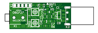
The PCB designed uses resistors and capacitors with 0805 SMD packaging. The size of the board is only 41.2 x 17.9 mm, which is practically dongle-sized. For the aerial an almost straight copper track has been placed at the edge of the board. In practice we achieved a range of about 6 metres (18 feet) with this. There is also room for a 5-way SIL header on the board. Here we find the inputs to the 3.5 mm jack plug, the input to P1 and the supply voltage. The latter permits the circuit to be powered independently from the mains supply, via for example three AA batteries or a Lithium button cell. Inductor L1 in the prototype is a type made by Murata that has a fairly high Q factor: minimum 60 at 100 MHz.

usb to fm transmitter pcb layout
Layout PCB USB FM transmitter

Take care when you solder filter choke L2, since the connections on both sides are very close together. The supply voltage is connected to this, so make sure that you don’t short out the USB supply! Use a resistance meter to check that there is no short between the two supply connectors before connecting the circuit to a USB port on a computer or to the batteries.

P1 has the opposite effect to what you would expect (clockwise reduces the volume), because this made the board layout much easier. The deviation and audio bandwidth varies with the setting of P1. The maximum sensitivity of the audio input is fairly large. With P1 set to its maximum level, a stereo input of 10 mVrms is sufficient for the sound on the radio to remain clear. This also depends on the setting of the VCO. With a higher tuning voltage the input signal may be almost twice as large (see VCO tuning curve in the data sheet). Above that level some audible distortion becomes apparent. If the attenuation can’t be easily set by P1, you can increase the values of R1 and R2 without any problems.

Measurements with an RF analyzer showed that the third harmonic had a strong presence in the transmitted spectrum (about 10 dB below the fundamental frequency). This should really have been much lower. With a low-impedance source connected to both inputs the bandwidth varies from 13.1 kHz (P1 at maximum) to 57 kHz (with the wiper of P1 set to 1/10).

In this circuit the pre-emphasis of the input is missing. Radios in Europe have a built-in de-emphasis network of 50 μs (75 μs in the US). The sound from the radio will therefore sound noticeably muffled. To correct this, and also to stop a stereo receiver from mistakenly reacting to a 19 kHz component in the audio signal, an enhancement circuit Is published elsewhere in this issue (Pre-emphasis for FM Transmitter, also with a PCB). Author: Mathieu Coustans, Elektor Magazine, 2009

MP3 FM Transmitter Parts List

Resistors (all SMD 0805)
R1,R2 = 22kΩ
R3 = 4kΩ7
R4,R5 = 1kΩ
R6 = 270Ω
P1 = 10kΩ preset, SMD (TS53YJ103MR10 Vishay Sfernice, Farnell # 1557933)
P2 = 100kΩ preset, SMD(TS53YJ104MR10 Vishay Sfernice, Farnell # 1557934)


Capacitors (all SMD 0805)
C1,C2,C5 = 4μF7 10V
C3,C8 = 100nF
C4,C7 = 2nF2
C6 = 470nF

Inductors
L1 = 390nF, SMD 1206 (LQH31HNR39K03L Murata, Farnell # 1515418)
L2 = 2200Ω @ 100MHz, SMD, common-mode choke, 1206 type(DLW31SN222SQ2L Murata, Farnell #1515599)

Semiconductors
IC1 = MAX2606EUT+, SMD SOT23-6 (Maxim Integrated Products)

Miscellaneous
K1 = 3.5mm stereo audio jack SMD (SJ1-3513-SMT
CUI Inc, DIGI-Key # CP1-3513SJCT-ND)
K2 = 5-pin header (only required in combination with 090305-I pre-emphasis circuit)
K3 = USB connector type A, SMD (2410 07 Lumberg, Farnell # 1308875)

Notice. The use of a VHF FM transmitter, even a low power device like the one described here, is subject to radio regulations and may not be legal in all countries.


source [ Link ]
Read More..