Showing posts with label and. Show all posts

Friday, December 20, 2013

Build a High And Low Voltage Cut Off With Time Delay Circuit Diagrams

The power line fluctuations and cut-offs cause damages to electrical appliances connected to the line. It is more serious in the case of domestic appliances like fridge and air conditioners. If a fridge is operated on low voltage, excessive current flows through the motor, which heats up, and get damaged.

The under/over voltage protection circuit with time delay presented here is a low cost and reliable circuit for protecting such equipments from damages. Whenever the power line is switched on it gets connected to the appliance only after a delay of a fixed time. If there is hi/low fluctuations beyond sets limits the appliance get disconnected. The system tries to connect the power back after the specific time delay, the delay being counted from the time of disconnection. If the power down time (time for which the voltage is beyond limits) is less than the delay time, the power resumes after the delay: If it is equal or more, then the power resumes directly.

This circuit has been designed, built and evaluated by me to use as a protector for my home refrigerator. This is designed around readily available semi-conductor devices such as standard bipolar medium power NPN transistor (D313/SL100/C1061), an 8-pin type 741 op-amp and NE555 timer IC. Its salient feature is that no relay hunting is employed. This draw back is commonly found in the proctors available in the market.

The complete circuit is consisting of various stages. They are: - Dual rail power supply, Reference voltage source, Voltage comparators for hi/low cut offs, Time delay stage and Relay driver stage. Lets now look at the step-by-step design details.

Dual rail power supply.
This is a conventional type of power supply as shown in Figure 1. The power is applied through the step-down transformer (230/12-0-12V/500mA). The DC proportional to the charging input voltage is obtained from bridge rectifier. Two electrolytics are there to bypass any spikes present. Bridge is capable of handling currents up to 1 Amp.
Output is given by: -
V(out) = 0.71 X V (secondary)
= 0.71 X 24V
= 17.04 V
(This equation is similar for the negative rail as well)

Circuit diagram

Build a High And Low Voltage Cut Off With Time Delay


Low voltage cut off op-amp
Figure 2 shows the use of very common and easily available op-amp 741 as a comparator. The op-amp is available in TO-5 and DIP type packing.

Circuit diagram

Build a High And Low Voltage Cut Off With Time Delay2


In this ckt the zener diode D1 and it’s associated resistor R1 are connected to the non-inverting terminal (+ve) of 741 to give the suitable reference voltage. The DC voltage from the sensor is given to the inverting (-ve) terminal through pre-set R2.This is used to set the input level.
When the sensor input is less than Zener voltage the output from the Op-amp remains high and when it is greater than Zener voltage the output goes low. When the sensing voltage is equal to Zener voltage the output of the op-amp is approximately zero.
This phenomenon is used as a decision for switching the relay and to give cutoff in a low voltage situation.

High voltage cut off op-amp
Here the op-amp is used as a inverted amplifier. See Figure 3.Zener and resistor network gives reference voltage to the inverting terminal (-ve) of op-amp. Sensing voltage derived through the 10 K pre-set is given to the non- inverting (+ve) terminal and this sets the high level cut.

When the input DC from the sensor is less than Zener voltage the output of the op-amp is low and vice-versa. When the input DC voltage is equal to the zener voltage, the op-amps output is approximately zero.

Circuit diagram

Build a High And Low Voltage Cut Off With Time Delay3


Time delay
I’ve selected the 555 timer due to following reasons.
1. Timing from microseconds through hours.
2. Ability to operate from wide range of supply voltages.
3. High temperature stability.
4. Easily Available.
5. Its triggering circuit is quite sensitive.

This is basically a monostable. The external timing capacitor C2 is held initially discharged by the timer. The circuit triggers upon receiving a pulse to its pin 2 when the level reaches 1/3 Vcc. Once triggered., the circuit will remain in that state until the set time is elapsed or power to the circuit cuts off. The delayed period in seconds is 1.1 C2.R1 where R1 is in megohms and C2 is in microfarads. In practice, R1 should not exceed 20 M. If you use an electrolytic capacitor for C2, select a unit for low leakage. The time delay may have to be adjusted by varying R1 to compensate for the wide tolerance of electrolytics.

Circuit diagram

Build a High And Low Voltage Cut Off With Time Delay


Relay Driver
The output from the voltage level detectors cannot directly drive the relay and hence the relay driver is used.

Circuit diagram

Build a High And Low Voltage Cut Off With Time Delay5


In this a relay (12V <500 ohms) is connected to the collector of NPN transistor. The out put voltage from the comparator is applied to the base of NPN transistor through a resistance R1. When the output from the comparator is low the transistor is in OFF state and the relay is in de-energized state. Similarly when the output from the comparator goes high the transistor switches ON and the flow of current from the collector to emitter of transistor energizes the relay.

Generally in a relay driver circuit, parallel to the relay coil, a diode or a capacitor is used. This is to eliminate the back e.m.f generated by the relay coil when currents are suddenly broken. Capacitor C1 is connected in parallel to the coil, which filters out the back emf but it, slows down the working of relay.

A better method is to connect two diodes (as shown in the figure 5) that stop the relay – transistor junction swinging more than 600mV above the positive rail or below the zero-volt rail. During normal operation the diodes are reverse biased and have no effect on the performance of circuit. But when back emf is induced, the diodes conduct heavily and absorb all transient voltages. However, I have employed the both methods.
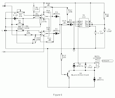
The Complete Circuit

Circuit diagram

Build a High And Low Voltage Cut Off With Time Delay1


Under normal operating conditions i.e. when the input voltage is between maximum and minimum limit the output from the both the comparators are low. The transistor Q1 is OFF and the relay is in de-energized (pole connected to N/C pin) state and the output is obtained.

When the input voltage is below or above the limits set by the pre-sets R8 or R9, the output of the Op-Amps goes either low or high and diodes D1 or D2 would be forward biased depending on the situation. Transistor Q1 switches ON and the flow of current from collector to emitter energizes the relay and the output is cutoff.

A small amount of hystersis has been added via feed back resistors R10 & R11 so that the relay turns on when the level falls to a particular value but does not turn again until it raises a substantial amount above this value. Other wise the relay contacts will frequently turn on/off and produce chattering.

Construction Hints
1) I used a piece of varoboard, which has copper strips on one side to mount the components, and housed the entire circuit and the transformer in a discarded ATX PC power supply box.

2) An autotransformer has been used to set the limits. Set the output of the autotransformer to 250V AC and connect it to the primary of transformer T1 (see Figure 1). Then adjust the pre-set R9 such that relay just energizes. This is the high limit. Next set the output of the autotransformer to 200V AC and adjust the pre-set R8 such that the relay energizes. Please note that these are my preferred limits but you may select any range from say 170 to 270V AC.

3) A neon with a suitable resistor could be connected between the AC supply lines as an ON indicator. Alternatively, LED with a current limiting resistor could be connected between the relay coil so when the relay is energized LED will indicate the situation.
Read More..

Wednesday, June 12, 2013

60 Watt Guitar Amplifier circuit and explanation

Bass, Treble, Harmonic modifier and Brightness controls
Output power: 40W into 8 Ohm and 60W into 4 Ohm loads

This design adopts a well established circuit topology for the power amplifier, using a single-rail supply of about 60V and capacitor-coupling for the speaker(s). The advantages for a guitar amplifier are the very simple circuitry, even for comparatively high power outputs, and a certain built-in degree of loudspeaker protection, due to capacitor C8, preventing the voltage supply to be conveyed into loudspeakers in case of output transistors failure. The preamp is powered by the same 60V rails as the power amplifier, allowing to implement a two-transistors gain-block capable of delivering about 20V RMS output. This provides a very high input overload capability.

Amplifier circuit diagram:
60 Watt Guitar Amplifier circuit schematic
60 Watt Guitar Amplifier Circuit Diagram
Amplifier parts:

R1__________________6K8 1W Resistor
R2,R4_____________470R 1/4W Resistors
R3__________________2K 1/2W Trimmer Cermet
R5,R6_______________4K7 1/2W Resistors
R7________________220R 1/2W Resistor
R8__________________2K2 1/2W Resistor
R9_________________50K 1/2W Trimmer Cermet
R10________________68K 1/4W Resistor
R11,R12______________R47 4W Wirewound Resistors
C1,C2,C4,C5________47µF 63V Electrolytic Capacitors
C3________________100µF 25V Electrolytic Capacitor
C6_________________33pF 63V Ceramic Capacitor
C7_______________1000µF 50V Electrolytic Capacitor
C8_______________2200µF 63V Electrolytic Capacitor (See Notes)
D1_________________LED Any type and color
D2________Diode bridge 200V 6A
Q1,Q2____________BD139 80V 1.5A NPN Transistors
Q3_____________MJ11016 120V 30A NPN Darlington Transistor (See Notes)
Q4_____________MJ11015 120V 30A PNP Darlington Transistor (See Notes)
SW1_______________SPST Mains switch
F1__________________4A Fuse with socket
T1________________220V Primary, 48-50V Secondary 75 to 150VA Mains transformer (See Notes)
PL1_______________Male Mains plug
SPKR______________One or more speakers wired in series or in parallel Total resulting impedance: 8 or 4 Ohm Minimum power handling: 75W


Preamplifier circuit diagram:
guitar preamplifier circuit schematic
Guitar Preamplifier Circuit Diagram
Preamplifier parts:

P1,P2______________10K Linear Potentiometers
P3_________________10K Log. Potentiometer
R1,R2______________68K 1/4W Resistors
R3________________680K 1/4W Resistor
R4________________220K 1/4W Resistor
R5_________________33K 1/4W Resistor
R6,R16______________2K2 1/4W Resistors
R7__________________5K6 1/4W Resistor
R8,R21____________330R 1/4W Resistors
R9_________________47K 1/4W Resistor
R10_______________470R 1/4W Resistor
R11_________________4K7 1/4W Resistor
R12,R20____________10K 1/4W Resistors
R13_______________100R 1/4W Resistor
R14,R15____________47R 1/4W Resistors
R17,R18,R19_______100K 1/4W Resistors
C1,C4,C5,C6________10µF 63V Electrolytic Capacitors
C2_________________47µF 63V Electrolytic Capacitor
C3_________________47pF 63V Ceramic Capacitor
C7_________________15nF 63V Polyester Capacitor
C8_________________22nF 63V Polyester Capacitor
C9________________470nF 63V Polyester Capacitor
C10,C11,C12________10µF 63V Electrolytic Capacitors
C13_______________220µF 63V Electrolytic Capacitor
D1,D2____________BAT46 100V 150mA Schottky-barrier Diodes (see Notes)
Q1,Q3____________BC546 65V 100mA NPN Transistors
Q2_______________BC556 65V 100mA PNP Transistor
J1,J2___________6.3mm. Mono Jack sockets
SW1,SW2___________SPST Switches

Sensitivity:
35mV input for 40W 8 Ohm output
42mV input for 60W 4 Ohm output
Frequency response:
50Hz to 20KHz -0.5dB; -1.5dB @ 40Hz; -3.5dB @ 30Hz
Total harmonic distortion @ 1KHz and 8 Ohm load:
Below 0.1% up to 10W; 0.2% @ 30W
Total harmonic distortion @ 10KHz and 8 Ohm load:
Below 0.15% up to 10W; 0.3% @ 30W
Total harmonic distortion @ 1KHz and 4 Ohm load:
Below 0.18% up to 10W; 0.4% @ 60W
Total harmonic distortion @ 10KHz and 4 Ohm load:
Below 0.3% up to 10W; 0.6% @ 60W
Treble control:
+9/-16dB @ 1KHz; +12/-24dB @ 10KHz
Brightness control:
+6.5dB @ 500Hz; +7dB @ 1KHz; +8.5dB @ 10KHz
Bass control:
-17.5dB @ 100Hz; -26dB @ 50Hz; -28dB @ 40Hz

Notes:
  • The value listed for C8 is the minimum suggested value. A 3300µF capacitor or two 2200µF capacitors wired in parallel would be a better choice.
  • The Darlington transistor types listed could be too oversized for such a design. You can substitute them with MJ11014 (Q3) and MJ11013 (Q4) or TIP142 (Q3) and TIP147 (Q4).
  • T1 transformer can be also a 24 + 24V or 25 + 25V type (i.e. 48V or 50V center tapped). Obviously, the center-tap must be left unconnected.
  • D1 and D2 can be any Schottky-barrier diode types. With these devices, the harmonic modifier operation will be hard. Using for D1 and D2 two common 1N4148 silicon diodes, the harmonic modifier operation will be softer.
  • In all cases where Darlington transistors are used as the output devices it is essential that the sensing transistor (Q2) should be in as close thermal contact with the output transistors as possible. Therefore a TO126-case transistor type was chosen for easy bolting on the heatsink, very close to the output pair.
  • R9 must be trimmed in order to measure about half the voltage supply across the positive lead of C7 and ground. A better setting can be done using an oscilloscope, in order to obtain a symmetrical clipping of the output wave form at maximum output power.
  • To set quiescent current, remove temporarily the Fuse F1 and insert the probes of an Avo-meter in the two leads of the fuse holder.
  • Set the volume control to the minimum and Trimmer R3 to its minimum resistance.
  • Power-on the circuit and adjust R3 to read a current drawing of about 30 to 35mA.
  • Wait about 15 minutes, watch if the current is varying and readjust if necessary.
Author: www.redcircuits.com
Read More..

Wednesday, May 29, 2013

OR AND NOR GATE SIgns

http://www.freeclipartnow.com/d/40920-1/circuit-elements.jpg
I think this signs will be so useful for the beginners who engage in electronics.Because most of them dont know the correct signs.Specially this will be a great advantage for the students who study in schools.
Read More..

Friday, April 12, 2013

Variable Voltage and Current Power Supply Circuit Using LM1458

This is another design for power supply that can build or based on LM1458. This is called variable voltage and current power supply. It is a once of regulated power supply. This figure below is shown the circuit;


The operation of this circuit is the power transformer requires an additional winding to supply the op-amps with a bipolar voltage (+/- 8 volts), and the negative voltage is also used to generate a reference voltage below ground so that the output voltage can be adjusted all the way down to 0. Current limiting is accomplished by sensing the voltage drop across a small resistor placed in series with the negative supply line. As the current increases, the voltage at the wiper of the 500 ohm pot rises until it becomes equal or slightly more positive than the voltage at the (+) input of the op amp.

Current limiting range is about 0 - 3 amps with components shown. The TIP32 and 2N3055 pass transistors should be mounted on suitable heat sinks and the 0.2 ohm current sensing resistor should be rated at 2 watts or more. The op amp output then moves negative and reduces the voltage at the base of the 2N3053 transistor which in turn reduces the current to the 2N3055 pass transistor so that the current stays at a constant level even if the supply is shorted. The heat produced by the pass transistor will be the product of the difference in voltage between the input and output, and the load current.

Read More..

Tuesday, April 9, 2013

Small Audio Amplifiers Using LM386 and NE5534

Many electronic projects require the use of a small audio amplifier. Be it a radio transceiver, a digital voice recorder, or an intercom, they all call for an audio amp that is small, cheap, and has enough power to provide adequate loudness to fill a room, without pretending to serve a disco! About one Watt RMS seems to be a convenient size, and this is also about the highest power that a simple amplifier fed from 12V can put into an 8 Ohm speaker. A very low saturation amplifier may go as high up as 2 Watt, but any higher power requires the use of a higher voltage power supply, lower speaker impedance, a bridge circuit, or a combination of those.

During my many years building electronic things I have needed small audio amps many times, and have pretty much standardized on a few IC solutions, first and and foremost the LM386, which is small, cheap, and very easy to use. But it does not produce high quality audio... For many applications, the advantages weigh more than the distortion and noise of this chip, so that I used it anyway. In other cases I used different chips, which perform better but need more complex circuits. Often these chips were no longer available the next time I needed a small amplifier.

When I last upgraded my computer, I replaced the old and trusty Soundblaster AWE 32 by a Soundblaster Audigy. The new card is better in many regards, but while the old one had an internal audio power amplifier, the new one doesnt! Thats bad news, because I have some pretty decent speakers for the PC, which are fully passive. So, I built a little stereo amp using two LM386 chips and installed it inside the computer, fed by the 12V available internally.

But then I wasnt satisfied. The LM386 might be suitable for "communication quality" audio, which is roughly the fidelity you get over a telephone, but for music its pretty poor! The distortion was awful. So, the day came when I decided to play a little more scientifically with small audio amps, looking for a way to get good performance with simple and inexpensive means.

I set up a test bench with a sine wave oscillator running at 1 kHz, an 8 Ohm speaker, 12V power supply, and the computer with the soundcard and Fast Fourier Transform software. One channel was connected to the oscillator together with the amplifier input, the other channel to the output and speaker. With this setup I measured the harmonic content of the audio signals. I did the tests at an output level of 0.1W, which is typical for moderately loud sound from a reasonably efficient speaker. Also, I used a music signal from a CD player to test the actual sound of each amplifier.

Circuit Project: Small Audio Amplifiers Using LM386 and NE5534

As already said above, the main attraction of the LM386 is the extreme simplicity of its application circuit. You can even eliminate R1 if the signal source is DC-grounded. If the speaker leads are long, you should add an RC snubber across the output to aid stability. Additionally, if you need higher gain (not necessary if the input is at line level), you can connect a 10uF capacitor between pins 1 and 8. Thats about all there is to it.

Now the bad news: This circuit produced a very high level of distortion! The second harmonic measured just -28dB from the main output. The third harmonic was at -35dB, while the noise level was at -82dB. There were assorted high harmonics at roughly -45dB. With music, the distortion was really disturbing, and also the noise level was uncomfortably high. The power supply rejection is poor, so that some hum and other supply noise gets through. In short, this was a lousy performance!

Since I had used so many LM386s in my projects, I had several different variations. In my material box I found a slightly newer LM386N-1. So I plugged it into my test amplifier. It was even worse! The second harmonic was at -24dB, the third harmonic at -31dB, while the noise was a tad better at -84dB. Folks, thats a total harmonic distortion of almost 7%! And the 0.1W output level at which this was measured is where such a circuit is about at its best...  The distortion can be plainly seen on the oscilloscope, and a visibly distorted waveform is about the most offending thing an audio designer can ever see!

Looking through my projects, I found one where I had used a GL386 chip. This is just a 386 made by another company. I unsoldered it and put it in my test amplifier. Surprise! It was dramatically better, with the second harmonic at -45dB, and the third at -57dB! The noise floor was -84dB, just like the LM386N-1. But even this level of distortion was plainly audible when listening to music. Thats roughly 0.6% THD. Some folks may consider it acceptable for music. I dont, but for communication equipment its fine. At this point, I decided to see if I could build a better amplifier, that doesnt become too complex nor expensive.

Circuit Project: Small Audio Amplifiers Using LM386 and NE5534

This was the first attempt. A low distortion, fast slew rate, but easy to find and rather inexpensive operational amplifier, driving a simple source follower made of two small transistors. These transistors are not biased, so they work at zero quiescent current, in full class B. The only mechanism that works against crossover distortion here is the high slew rate of the OpAmp, which is able to make the distortion bursts during crossover very short. To say the truth, I didnt expect to get usable performance from this circuit, and was really surprised when it worked much better than the 386! The second harmonic was at -77dB, the third at -79dB!

Also there were many high harmonics at roughly -84dB. That means a THD of about 0.015%.  The noise floor was down at the -120dB level! The power supply rejection was excellent, with no detectable feedtrough. Playing music, this amplifier sounded really good: No audible noise, and the distortion could be heard when paying attention to it, but I doubt that the average person would detect it! Not bad, for a bias-less design!

Just to see how important the slew rate of the OpAmp is, I pulled out the NE5534 and replaced it by a humble 741, which is many times slower. The result was dramatic: The second harmonic still good at -70dB, but the third harmonic was much worse, at -48dB. Also there were many high harmonics at the same -48dB level. Given that second harmonic distortion doesnt sound bad to most people, but third harmonic does, and high harmonics are even worse, it came as no surprise that the amplifier with the 741 sounded bad.

At low volume it sounded particularly bad! So I returned to the oscillator and measurement setup, testing at lower output power, and found that while the second and third harmonics followed the output, the high harmonics stayed mostly constant! So, at very low output, the high harmonics became very strong relative to the output. All this is the effect of the slower slew rate of the 741, which makes it less effective correcting the crossover distortion of the unbiased transistors. Interestingly, the noise floor of the 741 circuit wasnt bad: -118dB.

Just for fun, I tried this circuit with a third OpAmp: The TL071, which is good, but not as good as the 5534. The results: Second harmonic at -72dB, third and the high ones at -60dB, and the noise at -120dB. Its interesting that the second harmonic is much more suppressed than the third one. That must be a balancing effect of the symmetric output stage, and the better symmetry in the TL071 compared to other OpAmps.

Its worthwhile to note that this amplifier can be simplified a lot by using a split power supply. R1, R2, C1, C2 and C4 would be eliminated! But then you need the capacitor removed from C4 to bypass the negative supply line. The positive input of the chip goes to ground, while pin 4 and the collector of Q2 go to the negative supply. The rest stays the same. If you use a +-15V supply, the available RMS output power grows to over 10 Watt! Of course, you then need larger transistors. And since larger transistors are slower, the distortion will rise somewhat. An added benefit of a split supply is that the popping noise when switching on and off is eliminated.

Circuit Project: Small Audio Amplifiers Using LM386 and NE5534

As the next experiment, I decided to get rid of the crossover distortion. For this purpose, I added a traditional adjustable bias circuit with a transistor and a trimpot. Now I also had to add a current source, because with the bias circuit there is no single point into which the OpAmp could put its drive current into both bases! I adjusted the bias for the best distortion, and this was really  a good one! The second harmonic was down right where the test oscillator delivered it, about -80dB, so I couldnt really measure it!

The third harmonic was at -84dB, and the best improvement was that the higher harmonics had simply disappeared! They were all below the noise floor, which stayed at -120dB. Actually, this noise floor seems to come from the soundcard A/D converter, so that the actual noise of this and the above amplifier may even be better! With music, this amplifier sounded perfect - clean and smooth. And Im pretty confident that the THD is well below the limits of my measurement setup, which is 0.01%.

The quiescent current was around 10mA. When lowering it to about 3mA, the high harmonics started to rise out of the noise floor. If you want to adjust the bias for the exact best quiescent current, there is a simple trick: Lift R4 from the output, and connect it to pin 6. Now the output stage has been left outside the feedback loop, and all its distortion will show up at the output. Watching the signal on an oscilloscope, or even better on a real time spectrum analyzer (soundcard and software), adjust the trimpot to the lowest distortion level.

Have a current meter in the supply line and make sure that you dont exceed 30mA or so of quiescent current, in order to keep the small transistors cool. But most likely the best distortion will be at a current lower than that. Once the adjustment is complete, return R4 to its normal position. Now the full gain and slew rate of the operational amplifier is used to correct the small remaining cross-over distortion of the output stage, and the distortion will certainly disappear from the scope screen, from your ears, and possibly fall below the detection level of the spectrum analyzer!

This circuit can also be run from a split power supply, by exactly the same mods as for the previous circuit. And since the transistors are properly biased, there isnt any significant distortion increase when using larger transistors. Be sure to use some that have enough gain - you have only a few mA of driving available, and with a +-15V power supply and an 8 Ohm speaker, there can be almost 2A of output current! So, you need a gain of 300 at least. There are power transistors in the 4A class that provide such gain, and these are good candidates. The other option is using Darlington transistors, which far exceed the gain needed here. But they will again increase the distortion, not very much, but perhaps enough to make it audible again.

Read More..

Saturday, April 6, 2013

PbS and PbSe detectors

PbS and PbSe detectors
Cal Sensors has two new families of lead salt infrared detectors as well as the introduction of a new digital drive board. The new single channel detector (SCD) and multichannel detector (MCD) families provide sensitivity for a variety of infrared sensing applications.


The SCD-13HV (single channel detector- high-value) PbS detectors are designed to meet requirements for high volume, cost-sensitive applications. SCD detectors provide sensitivity with typical D* from 9 x 10¹⁰ to 1.75 x 10¹¹ Jones across the one to three micron wavelength range. Performance varies with element size and window type.


PbS and PbSe detectors

All SCD-13HV products support a glass window or lens configuration. Three element sizes are available in industry standard packages for easy integration. For applications where size is critical, such as portable test equipment, the SCD-13HV line offers a 1 by 1 mm detector in a TO-46 can. Where greater field-of-view or larger element sizes are important, 2 and 3 mm square detector sizes are available in TO-5 packages.

The new PbS and PbSe multi-channel detectors (MCD) provide sensitivity of 1.5 x 10¹⁰ Jones for detection of up to four distinct materials/gases. Covering one to five microns, the MCD product family provides channel isolation of >99.5 percent and a TO-5 footprint. An optional integrated thermistor within the MCD package optimizes temperature compensation for measurement precision. Co-locating the temperature sensor and detector material in a hermetically-sealed TO-5 package ensures they both ‘feel the same temperature variations and reduce potential effects of external environmental factors.

The four channel configuration offers opportunities for cost reduction and design simplification minimizing the need for multiple individual detectors and complex optics. System costs and footprints can be reduced up to 60 percent versus alternative single-detector designs. The technology is well-suited for a variety of applications including industrial and medical gas analysis, as well as auto and aviation emissions testing. It is useful for environmental applications such as stack monitoring, greenhouse gas analysis and overseeing air quality in confined spaces including tunnels and underground structures.

Though customizable for different applications across the one to five micron infrared spectrum, the MCD-15 line is available in a standard four-channel configuration with four discrete optical bandpass filters. This configuration supports CO, CO2 and hydro-carbon (such as methane) gas analysis.

Cal Sensors new Digital Drive Board optimizes signal levels for Cal Sensor´s one to four channel detectors. Designed with a socket that accepts Cal Sensors standard one to four-channel detectors, the digital board provides all the electronics necessary to drive the sensor, digitize the output and connect via USB to a computer or microprocessor. Supporting PbS and PbSe detector technologies, these drive boards were created to accelerate prototyping and product development.


source:[link]
Read More..

APD Bias Supply and Current Monitor


This circuit is consists of two circuit but in the figure this circuit is combines. This is the figure of the circuit.


The programmable APD bias supply is as before, except that feedback comes via A2. A2, sensing after the 1kW current shunt, isolates the R1-R2 path loading, preventing it from influencing the shunt’s voltage drop. A2’s action also insures tight output regulation, despite the current shunt’s presence. The current monitor, measures across the 1kW current shunt, presenting its output in Q1’s drain line. As shown, the output has about 1kW output impedance, although either of the circuit output options may be employed.

When considering circuit operation, note that both amplifiers are powered by the charge pump’s high voltage output, with their V– pin returned to the “2/3 VOUT” point. This biasing permits the amplifiers to process high voltage signals, although the voltage across them never exceeds 30V.
Read More..

Adapter power supply and charger circuit

Basically adapter, power supply and charger circuit has a similar construction which consists of a transformer, rectifier (rectifier) and smoothing the voltage. For there is usually an additional power supply voltage stabilizer of voltage regulator IC LM series 78XX or 79XX .
Below is a schematic circuit adapter, power supply, or battery charger (for gadgets, mobile phones, MP4player, smartphone) that is equipped with a 5V voltage stabilizer:

adapter, power supply and charger circuit
Adapter, power supply and charger circuit

Read More..

Thursday, April 4, 2013

How to Calculate and Match an Inverter Circuit with Battery and Transformer

Making an inverter all by you can be definitely lot of fun. However if the results are not satisfactory can completely spoil the whole purpose of the project. Installing and configuring the various inverter parameter like the battery and the transformer to with the actual assembled circuit needs special care and attention for deriving optimal results from the assembly. The article broadly discusses how to calculate and match a battery and transformer wit the relevant circuit and also enlightens regarding the possible faults that might be encountered and the respective troubleshooting procedures.
The article enlightens the many newcomers with some of the important clues, which might be helpful while configuring an inverter circuit with the battery and the transformer, so that efficient and optimal results can be achieved.

Configuring Inverter Parameters

While making an inverter, two points must be broadly taken into account – the transformer must be rated twice the maximum load that is expected to be used with the inverter and the battery must be rated at 1/4 more than the transformer ratings.

For example, if the inverter is expected to work at 12 volts, with maximum loads of 200 watts, the transformer must be rated at least 500 watts, corresponding to 40 plus amperage, roughly (dividing 500 by 12), and the battery in turn must be rated at = ¼ multiplied by 40 = 10, therefore 40 + 10 = 50 AH (minimum).

After procuring all the necessary components as explained above, it would be important to get them checked for compatibility with one another.

Only the battery, which is one the most crucial member, hopefully will not require any prior checking, because the printed rating and the charged voltage conditions should be sufficient to prove its reliability. It is assumed here that the condition of the battery is good and it’s relatively new and “healthy.”

Next comes the transformer, which is another most important component of the inverter, surely needs a thorough technical assessment. It may be done as follows:


The rating of the transformer can be best checked in the reverse order, i.e. by connecting its higher voltage winding to the AC mains input and checking the opposite winding for the specified outputs.

If the current ratings of the lower voltage section are within the maximum limits of a regular multi-tester (DMM), then it may be checked by switching ON the above AC and connecting the meter (set at, say AC 20 Amp) across the relevant winding.


Hold the meter prods connected across the winding terminals for a couple of seconds to get the readings directly on the meter.

If the reading matches with the specified transformer current, or at least is close to it, means your transformer is OK. Lower readings would mean a bad or a wrongly rated transformer winding.

The assembled circuit broadly needs to be checked for proper oscillation outputs across the bases of the power transistors or the mosfets.

This may be done by connecting the circuit to the battery, but without including the transformer initially. The checking should be done using some good frequency meter or if possible using an oscilloscope.
If the above gadgets are not there with you, a crude testing can be performed using a pair of ordinary headphones. Connect the headphone jack to the bases of the relevant power transistors; you should get a strong humming sound in the headphones, confirming a sound functioning of the oscillator stages.

The above confirmations should be enough to prompt you to configure all the sections together.

Connect the transformer to the relevant transistor or the power devices terminals; make sure the power devices are correctly integrated with the oscillator stage.

Finally the battery may be connected to the power inputs of the above configuration, again do not forget to include an appropriately rated FUSE in series with the battery positive.

The output of the transformer now may be attached with the specified maximum load and the power may be switched ON.

If everything’s is wired up correctly, the load should start operating at its full fledged power, if not, then something’s wrong with the circuit stage.

Since the oscillator section was appropriately checked before the final installations, surely the fault may lie with the power device stage.


If the fault is associated with low power outputs, the base resistors may be tweaked for possible faults, or may be reduced by adding parallel resistors to their existing base resistors.


The results may be checked as discussed above, if the results are positive and if you find improvements in the power outputs, the resistors may be further modified as desired, until the expected power output is delivered.


However this may lead to further heating of the devices and due care must be observed to keep them under check by either including cooling fans or increasing the heatsink dimensions.


However if the fault is accompanied with blowing of the fuse would mean a definite short circuit somewhere in the power stage.

The problem may also indicate a wrongly connected power device, a blown-of power device due to a possible shorting between the power device’s output terminals or the any of the terminals that needs to be perfectly kept aloof of each other.

Having explained a few of the above possibilities while configuring an inverter optimally, a thorough knowledge regarding electronic becomes an absolute necessity from the part of the individual who may be involved with the construction, without which the proceeding with the project may somehow get jeopardized.
Read More..