Friday, December 27, 2013

Build a Pulse Charger for reviving tired Lead Acid batteries

If you own a motorcycle, a motor home, a caravan, a lawn mover, a day cruiser or maybe a vintage car you must at some point had to write off a lead acid battery. When a battery is improperly charged or allowed to self-discharge as occurs during non-use, sulphate crystals build up on the batterys plates. The sulphate preventing the battery from being fully charged and therefore it is unable to deliver its full capacity. When trying to charge a battery in this state it only gets hot and looses water, the gravity of the electrolyte is not increasing to its normal “full charge” state. 

 Pulse Charger for reviving tired Lead Acid batteries Circuit Diagram

Pulse Charger for reviving tired Lead Acid batteries


The only thing you do is killing the battery completely. If a battery has a resting voltage of at least 1.8 Volts/cell and no cells are shorted, desalination of its plates can be done. This circuit is an add-on and part for a modification of a normal charger and it takes care of the sulphate problem.

The project: get hold of an old charger, big or small it’s your choice depending on the size of batteries you normally handle (bigger is better). There are some tricks to boost the performance if you need it. Start by ripping out everything except the transformer and the rectifier. Some older chargers are equipped with fin rectifiers, which have high voltage drop and must be replaced. Replace with a rugged bridge rectifier that can cope with the amperes. All wiring on secondary should be short and heavy wire. The rectifier should be bolted to the chassis to keep cool. If the charger have a high/low switch it’s a bonus, if not you can in some cases add a few turns of wire on the secondary winding. 

The circuit; a 14-stage ripple counter and oscillator IC 4060 produce a pulse, which is the heartbeat of the circuit. The pulse is feed to the 555 timer that deicide the length of the active output. With the switch you can select long or short pulse output. The output of the 555 timer triggers the zero-cross opt isolator triac driver MOC 3041 via a transistor. This gives the charger transformer a soft start via the triac and the snubber circuit. A small power supply is necessary for the circuit and consists of T1 a transformer 15V 0.1A secondary, a bridge rectifier, a regulator and two caps. Because this project include a charger that is (X) the outcome can differ in performance from one case to another. However this do not mean that your project doesn’t work, but the efficiency can vary. Some notes the snubbercap is a high voltage AC type (X) and the resistors on the mains side is at least 0.5W type. Use a triac that can take 400V+ and 10A+, I use BTA 25.600 but this is overkill in most cases. No PCB sorry!

How it works:
Well the short version. The object is to get the cell voltage high enough for the sulphate to dissolve without boiling or melting the battery. This is achieved by applying higher voltage for shorter periods and let the battery rest for a while. The pulses on short range is about 0.5s on / 3s off and the long pulse range is 1.4s on / 2s off. These times can vary depending on component tolerances. Start on long pulse and if you discover “boiling” (more than with normal charging) in the electrolyte switch to short puls. Don’t leave the process unattended, at least until you know how your specific version of this project turns out. I built ver.1 of this circuit some 10 years ago and have experimented with it but I’m sure someone can improve it further.
Read More..

Thursday, December 26, 2013

Touch Switch II

This circuit uses a 555 timer as the bases of the touch switch. You can learn more about 555 timers in the Learning section on my site. When the plate is touched the 555 timer is triggered and the output on pin 3 goes high turning on the LED and the buzzer for a certain period of time. The time that the LED and the buzzer is on is based on the values of the capacitor and resistor connected to pin 6 & 7. The 10M resistor on pin 2 causes the the circuit to be very sensitive to the touch.

Read More..

Wednesday, December 25, 2013

Build a Single cell Charger Circuit Diagram

This Single cell Charger Circuit Diagram detects a full-charge state and automatically switches to a float condition —from 240 mA to 12 mA. The circuit uses the 555 timer.


 Build a Single cell Charger Circuit Diagram


Build a Single cell Charger Circuit Diagram
 
Read More..

Tuesday, December 24, 2013

Simple Low Power Car Stereo Amplifier

A simple low power car stereo amplifier circuit based on TDA 2003 is shown here. The circuit uses cheap, readily available components and it is very easy to construct. TDA2003 is an integrated car radio amplifier from ST Micro electronics that has a lot of good features like short circuit protection for all pins, thermal over range low harmonic distortion, low cross over distortion etc. 

Circuit diagram :

Simple Low Power Car Audio Amplifier-Circuit Diagram

 A simple low power car stereo amplifier Circuit Diagram


In the circuit given here each TDA2003 is wired as a mono amplifier operating from a 12V supply. Resistors R2 and R3 forms a feedback network that sets the amplifiers gain. C7 is the input DC de-coupling capacitor and C5 couples the speaker to the amplifiers output. C4 is used for improving the ripple rejection while C1 and C2 are employed for power supply filtering. C3 and R1 are used for setting the upper frequency cut-off. Network comprising of C6 and R4 is used for frequency stabilization and to prevent oscillation.

Notes.

  • Assemble the circuit on a good quality PCB.
  • Heat sinks are necessary for both ICs.
  • The circuit can be operated from 12V DC.
  • S1 is the ON/OFF switch
Read More..

Monday, December 23, 2013

Cheap 12V to 220V Inverter

Even though today’s electrical appliances are increasingly often self-powered, especially the portable ones you carry around when camping or holidaying in summer, you do still sometimes need a source of 230 V AC - and while we’re about it, why not at a frequency close to that of the mains? As long as the power required from such a source remains relatively low - here we’ve chosen 30 VA - it’s very easy to build an inverter with simple, cheap components that many electronics hobbyists may even already have.

Though it is possible to build a more powerful circuit, the complexity caused by the very heavy currents to be handled on the low-voltage side leads to circuits that would be out of place in this summer issue. Let’s not forget, for example, that just to get a meager 1 amp at 230 VAC, the battery primary side would have to handle more than 20 ADC!. The circuit diagram of our project is easy to follow. A classic 555 timer chip, identified as IC1, is configured as an astable multivibrator at a frequency close to 100 Hz, which can be adjusted accurately by means of potentiometer P1.

Cheap 12V to 220V Inverter Circuit diagram:


As the mark/space ratio (duty factor) of the 555 output is a long way from being 1:1 (50%), it is used to drive a D-type flip-flop produced using a CMOS type 4013 IC. This produces perfect complementary square-wave signals (i.e. in antiphase) on its Q and Q outputs suitable for driving the output power transistors. As the output current available from the CMOS 4013 is very small, Darlington power transistors are used to arrive at the necessary output current. We have chosen MJ3001s from the now defunct Motorola (only as a semi-conductor manufacturer, of course!) which are cheap and readily available, but any equivalent power Darlington could be used.

These drive a 230 V to 2 × 9 V center-tapped transformer used ‘backwards’ to produce the 230 V output. The presence of the 230 VAC voltage is indicated by a neon light, while a VDR (voltage dependent resistor) type S10K250 or S07K250 clips off the spikes and surges that may appear at the transistor switching points. The output signal this circuit produces is approximately a square wave; only approximately, since it is somewhat distorted by passing through the transformer. Fortunately, it is suitable for the majority of electrical devices it is capable of supplying, whether they be light bulbs, small motors, or power supplies for electronic devices.

PCB layout:
pcb-layout-12-volt-to-230-volt-invertor-circuit-diagram
PCB Layout For Cheap 12V to 220V Inverter Circuit Diagram

Parts List :
Resistors
R1 = 18k?
R2 = 3k3
R3 = 1k
R4,R5 = 1k?5
R6 = VDR S10K250 (or S07K250)
P1 = 100 k potentiometer
Capacitors
C1 = 330nF
C2 = 1000 µF 25V
Semiconductor
T1,T2 = MJ3001
IC1 = 555
IC2 = 4013
Miscellaneous
LA1 = neon light 230 V
F1 = fuse, 5A
TR1 = mains transformer, 2x9V 40VA (see text)
4 solder pins
Note that, even though the circuit is intended and designed for powering by a car battery, i.e. from 12 V, the transformer is specified with a 9 V primary. But at full power you need to allow for a voltage drop of around 3 V between the collector and emitter of the power transistors. This relatively high saturation voltage is in fact a ‘shortcoming’ common to all devices in Darlington configuration, which actually consists of two transistors in one case. We’re suggesting a PCB design to make it easy to construct this project; as the component overlay shows, the PCB only carries the low-power, low-voltage components.

The Darlington transistors should be fitted onto a finned anodized aluminum heat-sink using the standard insulating accessories of mica washers and shouldered washers, as their collectors are connected to the metal cans and would otherwise be short-circuited. An output power of 30 VA implies a current consumption of the order of 3 A from the 12 V battery at the ‘primary side’. So the wires connecting the collectors of the MJ3001s [1] T1 and T2 to the transformer primary, the emitters of T1 and T2 to the battery negative terminal, and the battery positive terminal to the transformer primary will need to have a minimum cross-sectional area of 2 mm2 so as to minimize voltage drop.

The transformer can be any 230 V to 2 × 9 V type, with an E/I iron core or toroidal, rated at around 40 VA. Properly constructed on the board shown here, the circuit should work at once, the only adjustment being to set the output to a frequency of 50 Hz with P1. You should keep in minds that the frequency stability of the 555 is fairly poor by today’s standards, so you shouldn’t rely on it to drive your radio-alarm correctly – but is such a device very useful or indeed desirable to have on holiday anyway? Watch out too for the fact that the output voltage of this inverter is just as dangerous as the mains from your domestic power sockets.

So you need to apply just the same safety rules! Also, the project should be enclosed in a sturdy ABS or diecast so no parts can be touched while in operation. The circuit should not be too difficult to adapt to other mains voltages or frequencies, for example 110 V, 115 V or 127 V, 60 Hz. The AC voltage requires a transformer with a different primary voltage (which here becomes the secondary), and the frequency, some adjusting of P1 and possibly minor changes to the values of timing components R1 and C1 on the 555.

Source: http://www.ecircuitslab.com/2011/08/cheap-12v-to-220v-inverter.html
Read More..

Sunday, December 22, 2013

Animal Friendiy Mousetrap

Animal Friendiy Mousetrap-Image
This mousetrap is built around a PlC12F683 and uses an infrared transmissive optical sensor that is modulated at a frequency of 38 kHz, so that it isnt affected by the ambient light. The modulation is carried out by the PlC, which generates a 38 kHz signal at port GP2, which is connected to the lR LED. The lR receiver is a type that is usually found for use with remote controls. lt reacts only to 38 kHz signals. lt reports the presence of an lR signal to the PIC via port GP1.


When the lR lightbeam is broken the PIC turns of the relay via port GP4 and FET T1 , which: causes the door of the mousetrap to close. The transmissive optical sensor is housed inside a small wooden box. A small amount of food is placed inside this box.

Animal Friendiy Mousetrap Circuit Diagram

Animal Friendiy Mousetrap-Circuit diagram

When a mouse walks through the light beam on its way to the food it causes the door to shut behind it and an LED starts flashing. The door is normally kept open by the coil of a relay that has been taken apart. When the coil is no longer powered the tin door is pushed shut by means of a spring. A piece of glass or transparent plastic should be put on top of the box, so that the mouse doesnt have to enter a dark space. When a mouse has been caught it can be let free again somewhere outside, some distance away from the house.

The reset button has to be pressed to ready the trap for its next victim. The author has managed to catch a few dozen mice with this device. The program is written in PICBASIC Pro and can be freely downloaded from the Elektor website, it is found in archive file # 100308-11.zip.

Read More..

Saturday, December 21, 2013

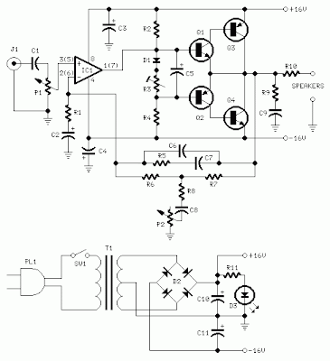
10 W Audio Amplifier Rise

This design is based on the 18 Watt Audio Amplifier, and was developed mainly to satisfy the requests of correspondents unable to locate the TLE2141C chip. It uses the widespread NE5532 Dual IC but, obviously, its power output will be comprised in the 9.5 - 11.5W range, as the supply rails cannot exceed ±18V.

10 W Audio Amplifier Circuit Diagram

10 W Audio Amplifier Circuit Diagram


As amplifiers of this kind are frequently used to drive small loudspeaker cabinets, the bass frequency range is rather sacrificed. Therefore a bass-boost control was inserted in the feedback loop of the amplifier, in order to overcome this problem without quality losses. The bass lift curve can reach a maximum of +16.4dB @ 50Hz. In any case, even when the bass control is rotated fully counterclockwise, the amplifier frequency response shows a gentle raising curve: +0.8dB @ 400Hz, +4.7dB @ 100Hz and +6dB @ 50Hz (referred to 1KHz).

Notes:

  • Can be directly connected to CD players, tuners and tape recorders.
  • Schematic shows left channel only, but C3, C4, IC1 and the power supply are common to both channels.
  • Numbers in parentheses show IC1 right channel pin connections.
  • A log type for P2 will ensure a more linear regulation of bass-boost.
  • Do not exceed 18 + 18V supply.
  • Q3 and Q4 must be mounted on heatsink.
  • D1 must be in thermal contact with Q1.
  • Quiescent current (best measured with an Avo-meter in series with Q3 Emitter) is not critical.
  • Set the volume control to the minimum and R3 to its minimum resistance.
  • Power-on the circuit and adjust R3 to read a current drawing of about 20 to 25mA.
  • Wait about 15 minutes, watch if the current is varying and readjust if necessary.
  • A correct grounding is very important to eliminate hum and ground loops. Connect to the same point the ground sides of J1, P1, C2, C3 &C4. Connect C9 to the output ground.
  • Then connect separately the input and output grounds to the power supply ground.

Parts:

P1_________________22K   Log.Potentiometer (Dual-gang for stereo)
P2________________100K Log.Potentiometer (Dual-gang for stereo)
R1________________820R 1/4W Resistor
R2,R4,R8____________4K7 1/4W Resistors
R3________________500R 1/2W Trimmer Cermet
R5_________________82K 1/4W Resistor
R6,R7______________47K 1/4W Resistors
R9_________________10R 1/2W Resistor
R10__________________R22 4W Resistor (wirewound)

C1,C8_____________470nF 63V Polyester Capacitor
C2,C5_____________100µF 25V Electrolytic Capacitors
C3,C4_____________470µF 25V Electrolytic Capacitors
C6_________________47pF 63V Ceramic or Polystyrene Capacitor
C7_________________10nF 63V Polyester Capacitor
C9________________100nF 63V Polyester Capacitor

D1______________1N4148 75V 150mA Diode

IC1_____________NE5532 Low noise Dual Op-amp

Q1_______________BC547B 45V 100mA NPN Transistor
Q2_______________BC557B 45V 100mA PNP Transistor
Q3_______________TIP42A 60V 6A PNP Transistor
Q4_______________TIP41A 60V 6A NPN Transistor

J1__________________RCA audio input socket

Power supply parts:

R11_________________1K5  1/4W Resistor

C10,C11__________4700µF 25V Electrolytic Capacitors

D2________________100V 4A Diode bridge
D3________________5mm. Red LED

T1________________220V Primary, 12 + 12V Secondary 24-30VA Mains transformer

PL1_______________Male Mains plug

SW1_______________SPST Mains switch
 

Technical data:

Output power:
10 Watt RMS into 8 Ohm (1KHz sinewave)
Sensitivity:
115 to 180mV input for 10W output (depending on P2 control position)
Frequency response:
See Comments above
Total harmonic distortion @ 1KHz:
0.1W 0.009% 1W 0.004% 10W 0.005%
Total harmonic distortion @ 100Hz:
0.1W 0.009% 1W 0.007% 10W 0.012%
Total harmonic distortion @ 10KHz:
0.1W 0.056% 1W 0.01% 10W 0.018%
Total harmonic distortion @ 100Hz and full boost:
1W 0.015% 10W 0.03%
Max. bass-boost referred to 1KHz:
400Hz = +5dB; 200Hz = +7.3dB; 100Hz = +12dB; 50Hz = +16.4dB; 30Hz = +13.3dB
Unconditionally stable on capacitive loads
 
Read More..

Friday, December 20, 2013

Build a High And Low Voltage Cut Off With Time Delay Circuit Diagrams

The power line fluctuations and cut-offs cause damages to electrical appliances connected to the line. It is more serious in the case of domestic appliances like fridge and air conditioners. If a fridge is operated on low voltage, excessive current flows through the motor, which heats up, and get damaged.

The under/over voltage protection circuit with time delay presented here is a low cost and reliable circuit for protecting such equipments from damages. Whenever the power line is switched on it gets connected to the appliance only after a delay of a fixed time. If there is hi/low fluctuations beyond sets limits the appliance get disconnected. The system tries to connect the power back after the specific time delay, the delay being counted from the time of disconnection. If the power down time (time for which the voltage is beyond limits) is less than the delay time, the power resumes after the delay: If it is equal or more, then the power resumes directly.

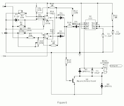
This circuit has been designed, built and evaluated by me to use as a protector for my home refrigerator. This is designed around readily available semi-conductor devices such as standard bipolar medium power NPN transistor (D313/SL100/C1061), an 8-pin type 741 op-amp and NE555 timer IC. Its salient feature is that no relay hunting is employed. This draw back is commonly found in the proctors available in the market.

The complete circuit is consisting of various stages. They are: - Dual rail power supply, Reference voltage source, Voltage comparators for hi/low cut offs, Time delay stage and Relay driver stage. Lets now look at the step-by-step design details.

Dual rail power supply.
This is a conventional type of power supply as shown in Figure 1. The power is applied through the step-down transformer (230/12-0-12V/500mA). The DC proportional to the charging input voltage is obtained from bridge rectifier. Two electrolytics are there to bypass any spikes present. Bridge is capable of handling currents up to 1 Amp.
Output is given by: -
V(out) = 0.71 X V (secondary)
= 0.71 X 24V
= 17.04 V
(This equation is similar for the negative rail as well)

Circuit diagram

Build a High And Low Voltage Cut Off With Time Delay


Low voltage cut off op-amp
Figure 2 shows the use of very common and easily available op-amp 741 as a comparator. The op-amp is available in TO-5 and DIP type packing.

Circuit diagram

Build a High And Low Voltage Cut Off With Time Delay2


In this ckt the zener diode D1 and it’s associated resistor R1 are connected to the non-inverting terminal (+ve) of 741 to give the suitable reference voltage. The DC voltage from the sensor is given to the inverting (-ve) terminal through pre-set R2.This is used to set the input level.
When the sensor input is less than Zener voltage the output from the Op-amp remains high and when it is greater than Zener voltage the output goes low. When the sensing voltage is equal to Zener voltage the output of the op-amp is approximately zero.
This phenomenon is used as a decision for switching the relay and to give cutoff in a low voltage situation.

High voltage cut off op-amp
Here the op-amp is used as a inverted amplifier. See Figure 3.Zener and resistor network gives reference voltage to the inverting terminal (-ve) of op-amp. Sensing voltage derived through the 10 K pre-set is given to the non- inverting (+ve) terminal and this sets the high level cut.

When the input DC from the sensor is less than Zener voltage the output of the op-amp is low and vice-versa. When the input DC voltage is equal to the zener voltage, the op-amps output is approximately zero.

Circuit diagram

Build a High And Low Voltage Cut Off With Time Delay3


Time delay
I’ve selected the 555 timer due to following reasons.
1. Timing from microseconds through hours.
2. Ability to operate from wide range of supply voltages.
3. High temperature stability.
4. Easily Available.
5. Its triggering circuit is quite sensitive.

This is basically a monostable. The external timing capacitor C2 is held initially discharged by the timer. The circuit triggers upon receiving a pulse to its pin 2 when the level reaches 1/3 Vcc. Once triggered., the circuit will remain in that state until the set time is elapsed or power to the circuit cuts off. The delayed period in seconds is 1.1 C2.R1 where R1 is in megohms and C2 is in microfarads. In practice, R1 should not exceed 20 M. If you use an electrolytic capacitor for C2, select a unit for low leakage. The time delay may have to be adjusted by varying R1 to compensate for the wide tolerance of electrolytics.

Circuit diagram

Build a High And Low Voltage Cut Off With Time Delay


Relay Driver
The output from the voltage level detectors cannot directly drive the relay and hence the relay driver is used.

Circuit diagram

Build a High And Low Voltage Cut Off With Time Delay5


In this a relay (12V <500 ohms) is connected to the collector of NPN transistor. The out put voltage from the comparator is applied to the base of NPN transistor through a resistance R1. When the output from the comparator is low the transistor is in OFF state and the relay is in de-energized state. Similarly when the output from the comparator goes high the transistor switches ON and the flow of current from the collector to emitter of transistor energizes the relay.

Generally in a relay driver circuit, parallel to the relay coil, a diode or a capacitor is used. This is to eliminate the back e.m.f generated by the relay coil when currents are suddenly broken. Capacitor C1 is connected in parallel to the coil, which filters out the back emf but it, slows down the working of relay.

A better method is to connect two diodes (as shown in the figure 5) that stop the relay – transistor junction swinging more than 600mV above the positive rail or below the zero-volt rail. During normal operation the diodes are reverse biased and have no effect on the performance of circuit. But when back emf is induced, the diodes conduct heavily and absorb all transient voltages. However, I have employed the both methods.
The Complete Circuit

Circuit diagram


Build a High And Low Voltage Cut Off With Time Delay1


Under normal operating conditions i.e. when the input voltage is between maximum and minimum limit the output from the both the comparators are low. The transistor Q1 is OFF and the relay is in de-energized (pole connected to N/C pin) state and the output is obtained.

When the input voltage is below or above the limits set by the pre-sets R8 or R9, the output of the Op-Amps goes either low or high and diodes D1 or D2 would be forward biased depending on the situation. Transistor Q1 switches ON and the flow of current from collector to emitter energizes the relay and the output is cutoff.

A small amount of hystersis has been added via feed back resistors R10 & R11 so that the relay turns on when the level falls to a particular value but does not turn again until it raises a substantial amount above this value. Other wise the relay contacts will frequently turn on/off and produce chattering.

Construction Hints
1) I used a piece of varoboard, which has copper strips on one side to mount the components, and housed the entire circuit and the transformer in a discarded ATX PC power supply box.

2) An autotransformer has been used to set the limits. Set the output of the autotransformer to 250V AC and connect it to the primary of transformer T1 (see Figure 1). Then adjust the pre-set R9 such that relay just energizes. This is the high limit. Next set the output of the autotransformer to 200V AC and adjust the pre-set R8 such that the relay energizes. Please note that these are my preferred limits but you may select any range from say 170 to 270V AC.

3) A neon with a suitable resistor could be connected between the AC supply lines as an ON indicator. Alternatively, LED with a current limiting resistor could be connected between the relay coil so when the relay is energized LED will indicate the situation.
Read More..

Thursday, December 19, 2013

Proximity Switch

This circuit is for an unusually sensitive and stable proximity alarm which may be built at very low cost. If the negative terminal is grounded, it will detect the presence of a hand at more than 200mm. If it is not grounded, this range is reduced to about one-third. The Proximity Switch emits a loud, falling siren when a body is detected within its range. A wide range of metal objects may be used for the sensor, including a metal plate, a doorknob, tin foil, a set of burglar bars — even a complete bicycle. Not only this, but any metal object which comes within range of the sensor, itself becomes a sensor.

Proximity Switch

For example, if a tin foil sensor is mounted underneath a table, metal items on top of the table, such as cutlery, or a dinner service, become sensors themselves. The touch plate connected to the free end of R1 detects the electric field surrounding the human body, and this is of a relatively constant value and can therefore be reliably picked up. R1 is not strictly necessary, but serves as some measure of protection against static charge on the body if the sensor should be touched directly. As a body approaches the sensor, the value of C1 effectively increases, causing the frequency of oscillator IC1.A to drop.

Consequently capacitor C2 has more time to discharge through P2, with the result that the inputs at IC1.B go Low, and the output goes High. As the output goes High, so C3 is charged through LED D2. D2 serves a dual purpose —namely as a visual indication of detection, and to lower the maximum charge on C3, thus facilitating a sharper distinction between High and Low states of capacitor C3. The value of R4 is chosen to enable C3 to discharge relatively quickly as pulses through D2 are no longer sufficient to maintain its charge. The value of C3 may be increased for a longer sounding of the siren, with a slight reduction in responsiveness at the sensor.

Proximity Switch circuit diagram

When C3 goes High, this triggers siren IC1.C and IC1.D. The two NAND gates drive piezo sounder X1 in push-pull fashion, thereby greatly increasing its volume. If a piezo tweeter is used here, the volume will be sufficient to make one’s ears sing. The current consumption of the circuit is so low a small 9-V alkaline PP3 battery would last for about one month. As battery voltage falls, so sensitivity drops off slightly, with the result that P1 may require occasional readjustment to maintain maximum sensitivity. On the down side of low cost, the hysteresis properties of the 4093 used in the circuit are critical to operation, adjustment and stability of the detector.

In some cases, particularly with extremely high sensitivity settings, it will be found that the circuit is best powered from a regulated voltage source. The PCB has an extra ground terminal to enable it to be easily connected to a large earthing system. Current consumption was measured at 3.5 mA stand-by or 7 mA with the buzzer activated. Usually, only P1 will require adjustment. P2 is used in place of a standard resistor in order to match temperature coefficients, and thus to enhance stability. P2 should be adjusted to around 50 k, and left that that setting.

Proximity Switch PCB
The circuit is ideally adjusted so that D2 ceases to light when no body is near the sensor. Multiturn presets must be used for P1 and P2. Since the piezo sounder is the part of the circuit which is least affected by body presence, a switch may be inserted in one of its leads to switch the alarm on and off after D2 has been used to check adjustment. Make sure that there is a secure connection between the circuit and any metal sensor which is used.


Resistors:
  • R1 = 10kΩ
  • R2 = 4kΩ7
  • R3 = 1kΩ
  • R4 = 47kΩ
  • R5 = 47kΩ
  • P1,P2 = 100kΩ multiturn cermet, horizontal
Capacitors:
  • C1,C2 = 22pF
  • C3 = 22µF 40V radial
  • C4 = 10nF
  • C5 = 100µF 25V radial
Semiconductors:
  • D1 = 1N4148
  • D2 = LED, red
  • IC1 = 4093
Miscellaneous:
  • BZ1 = AC buzzer
Read More..

Wednesday, December 18, 2013

Operational Amplifier Op Amp Basics

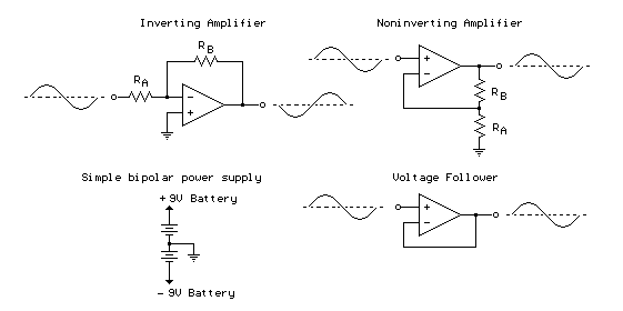
The op-amp is basically a differential amplifier having a large voltage gain, very high input impedance and low output impedance. The op-amp has a "inverting" or (-) input and "non-inverting" or (+) input and a single output. The op-amp is usually powered by a dual polarity power supply in the range of +/- 5 volts to +/- 15 volts. A simple dual polarity power supply is shown in the figure below which can be assembled with two 9 volt batteries.

Operational Amplifier (Op-Amp) Basics

Inverting Amplifier:


The op-amp is connected using two resistors RA and RB such that the input signal is applied in series with RA and the output is connected back to the inverting input through RB. The non-inverting input is connected to the ground reference or the center tap of the dual polarity power supply. In operation, as the input signal moves positive, the output will move negative and visa versa. The amount of voltage change at the output relative to the input depends on the ratio of the two resistors RA and RB.

As the input moves in one direction, the output will move in the opposite direction, so that the voltage at the inverting input remains constant or zero volts in this case. If RA is 1K and RB is 10K and the input is +1 volt then there will be 1 mA of current flowing through RA and the output will have to move to -10 volts to supply the same current through RB and keep the voltage at the inverting input at zero. The voltage gain in this case would be RB/RA or 10K/1K = 10. Note that since the voltage at the inverting input is always zero, the input signal will see a input impedance equal to RA, or 1K in this case. For higher input impedance, both resistor values can be increased.

Non-inverting Amplifier:


The non-inverting amplifier is connected so that the input signal goes directly to the non-inverting input (+) and the input resistor RA is grounded. In this configuration, the input impedance as seen by the signal is much greater since the input will be following the applied signal and not held constant by the feedback current. As the signal moves in either direction, the output will follow in phase to maintain the inverting input at the same voltage as the input (+). The voltage gain is always more than 1 and can be worked out from Vgain = (1+ RB/RA).

Voltage Follower:


The voltage follower, also called a buffer, provides a high input impedance, a low output impedance, and unity gain. As the input voltage changes, the output and inverting input will change by an equal amount.

Read More..

Tuesday, December 17, 2013

Belgian Earth Fault Detector

Having been affected by earth fault accidents,  the author put together this little circuit. It  consist of just three elements: the neon with its  original resistor for example, salvaged from  the switch on an AC power bar and a small  capacitor (class Y) salvaged from the electronics of a low-consumption lamp.

Belgian Earth Fault Detector Image

A larger capacitance makes the neon glow brighter. All this  for no money at all. The neon lights only when there is an efficient Earth present. This works  well at the author’s home, with Live or Neutral either way round. In the Elektor laboratory based in The Netherlands, some concerns  were expressed as described in the June 2011  issue [1], as the circuit was sensitive to the relative positions of the Live and Neutral. So the  Earth fault detector can also be used as a Phase  detector, but probably in Belgium only.

Belgian Earth Fault Detector-Circuit Diagram

The whole thing can easily be incorporated into a power socket; the author used a small transparent cover to protect the neon.

Note. As opposed to the UK and the US, some AC  power outlets in Belgium  and all in The  Netherlands are not polarized, i.e. AC power plugs (both earthed  and non-earthed) can be inserted either way around.

Source : http://www.ecircuitslab.com/2012/05/belgian-earth-fault-detector.html
Read More..

Monday, December 16, 2013

Home Made Metal Detector

This homemade metal detector circuit will help you find objects composed of materials with relatively high magnetic permeability. It is not suitable for buried coins discovery that is not sensitive enough but you can detect pirates treasures! The metal detector is powered by 2 x 9V batteries, each of it charges with 15mA. L1 detector coil is part of the sinusoidal oscillator built around transistor T1.

Normally, the center frequency of the voltage controlled oscillator (VCO) from the PLL loop that is contained in IC1 is equal to the oscillation frequency of T1. This changes when entering a metallic object (ferrous or nonferrous) in the field induced by L1. S1 is a miniature 2-pole switch. Meter needle deviation is a measure of frequency change, since the direction of deviation depends on the type of material detected by the coil. The meter tool used for this homemade metal detector is zero as central, +-50µA.

Metal detector circuit schematic


Coil L1 consists of 40 turns of enamelled copper wire, wound on a plastic template with a diameter of about 10 cm. Inductance thus obtained ensure the functioning of the oscillator at a frequency approximately equal to the VCO included in the PLL loop. Use an oscilloscope to check that pin 2 of IC1 delivers sinusoidal signal with frequency about 75 kHz.

Adjust P1 so that fronts rectangular signal from pin 4 to coincide with the peaks of the sinusoidal signal from pin 2. Then, adjust P2 in order to obtain 0 on the meter. Since the neutral zero setting “runs” with the battery’s decreasing voltage it will be necessary to restore it (zero balancing) from time to time during use of the metal detector.
Read More..